
Introduction
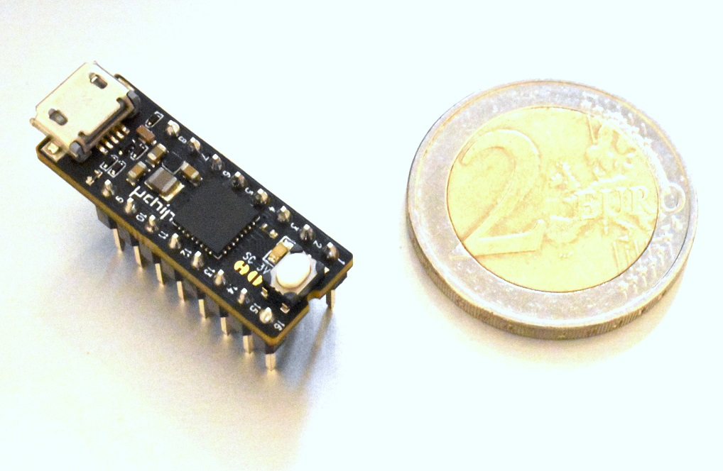
The Arduino Zero made quite popular the ATSAMD21 microcontroller, which was later adopter by a number of other compatible boards like Adafruit’s Feather M0 or Itaca-Innovation’s uChip.
The SAMD21 is a 48-MHz Cortex M0+, with hardware multiplier, a nice set of peripherals (including an USB Host/Device), an event system and DMA. In its higher-tier version, this MCU provides a good amount of memory for many applications, thanks to its 32 kB of RAM and 256 kB of Flash.
While the SAMD21 grants a decent amount of firepower, sometimes some MHz more would be indeed very useful. Furthermore, it is always interesting to see how much we can push these little beasts!
In a previous article, we already showed that some of the ATSAMD21 peripherals can be “overclocked”. In particular, we overclocked the SPI to achieve a better refresh rate. In this article, we test if is it possible to overclock the SAMD21 core itself (answer: yes!), how far we can push the speed, and what kind of code/external hardware modifications are required.
Some good news and some bad news
First the good news: the main CPU clock is produced by a complex internal circuitry that allows generating the desired frequency, by configuring some registers, so no hardware modifications are required.
Furthermore, for each peripheral we can set its working frequency, so that overclocking the CPU will not affect the operation of other peripherals, which might introduce undesired effects. This of course requires a careful configuration of all the clock subsystem.
Now the bad news: we need quite a good amount of code, especially if we need to use the USB too. Well, this is not a problem, as you will have to just copy and paste the final code.
As a last bad news, if you use the SysTick timer, then, overclocking the CPU will increase the SysTick clock frequency too. This might induce some issues, especially if you use the Arduino framework.
In fact, delays and timing functions (e.g. millis(), delay() and micros()) are based on the SysTick timer. For instance, by overclocking the CPU to 72 MHz, if you call “delay(1000);”, you get an actual delay of 666ms, because the CPU is going 50% faster. To overcome this effect, you should modify the variant.h file of your board, and set VARIANT_MCK to the actual clock frequency, i.e. 72000000 in this example. However, to avoid issues, creating a new variant would be preferable. We will cover the variant creation in a separate article.
Another solution, is to take into account the increased speed, and write delay(1500) instead of delay(1000) and multiplying by 1.5 the result of millis() and micros(). Actually, instead of multiplying by 1.5 we suggest this simple operation: time = micros(); time += (time >> 1). In this way, you will save a floating point multiplication.
Software
For this hack, we will use the Arduino IDE: of course, you do not need the Arduino framework, and you can use any IDE you want.
To test if our hack is successful, we will use a very simple method. We will measure the frequency at which one GPIO toggles. The sketch can be downloaded here.
Theory of operation.
In many modern high-speed CPU/MCU designs, the CPU clock is not directly generated by a crystal oscillator, which runs at the same frequency of the desired clock. Instead, the high-frequency clock is usually derived from a reference oscillator, which runs at a much lower frequency. This reference frequency is “multiplied” by precise factor, to achieve the desired frequency. The ATSAMD21 follows the same strategy. Its 48MHz operating frequency is derived from a much lower-frequency reference oscillator[1], which can be chosen by configuring some registers. The frequency of the chosen reference oscillator is then multiplied, to achieve the desired operating value.
But, how can we multiply frequency? We will not go too much into details, as this is beyond the scope of this article. However, we would like to give an intuitive explanation.
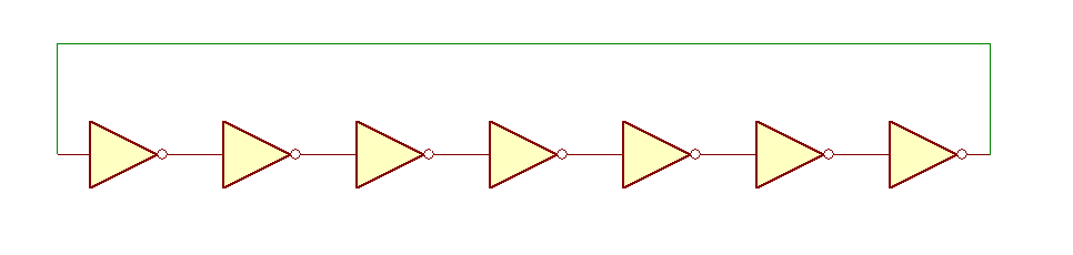
For today’s standards, making a relatively high-speed oscillator is not difficult. For instance, one can put in a loop an odd number of inverters. Each inverter has a finite speed, i.e. they introduce a small delay. You can easily see that, in this way, the system will start oscillating, as there is no stable condition (try putting a “high” logic level somewhere, and follow the signal!). The main issue of this technique is the poor precision of the achieved frequency, and its strong dependence on many factors. Slight variations of the temperature or operating voltage, could lead to huge variations of the generated frequency. Furthermore, even at the same operating conditions, there would be a huge variation between sample to sample.
However, following the previous example, if instead of using simple inverters, we introduce something that allows us to adjust the speed of such inverters, we can regulate the frequency. Yeah, useful, but this does not solve the problem of the frequency precision: one would have to measure the output frequency, and constantly adjusting the speed of such inverters! This is actually what it is internally done! Let us assume that we need a 100MHz stable output frequency, but we have only a 1-MHz reference clock. All we have to do is to use an “adjustable” oscillator. We then divide its output frequency by 100, using a simple counter. After that, we simply compare the output frequency with our 1-MHz reference frequency. If our 1-MHz reference frequency is faster than the frequency of the adjustable oscillator divided by 100, it means that our adjustable oscillator is running too slow. Therefore we ask it to go faster. On the opposite, if our 1-MHz reference is slower, then our oscillator is going too fast, therefore we ask it to go slower.
These systems are called FLL, frequency-locked loop, i.e. a system that tries to keep the output frequency (divided by the multiplication factor) locked to the reference value. A slightly different implementation is the PLL (phase-locked loop), i.e. a system that also tries to keep the generated signal in phase with the reference. The digital versions are called DFLL and DPLL.
The ATSAMD21 has both a DFLL (which can run at 48MHz, hence called DFLL48), and a DPLL (which can run at 96MHz, hence DPLL96).
The ATSAMD21 has also many clock sources and many “users” (CPU, BUS, peripherals), which can run at different frequencies. To accommodate the need of these different frequencies, the ATSAMD21 includes several GCLKs (generic clock generators). Each GCLK allows to divide an input clock by some desired factor. The input clock can be configured from a list of different sources. Furthermore, the output of a GCLK can be attached to one or more “users”.
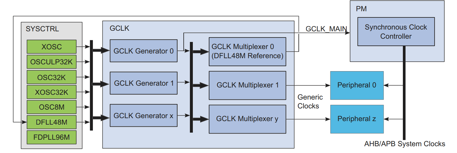
The program
The procedure is simple. The Arduino framework already configures the DFLL48 to run at 48MHz from the 32768 Hz crystal oscillator. This allows us to have a stable reference frequency for the DPLL96. We divide the 48MHz by 48, to achieve a 1-MHz reference value, using GCLK4. The 1-MHz frequency from the GCLK4 is fed to the DPLL96. Then, we configure the DPLL multiplier so that it will run at the desired CPU frequency. For instance, if we set the multiplier to 60 (actual value written to the register: 59), we run the CPU at 60 MHz. After that, we configure the DPLL as the clock source for the GCLK0, which is used as the CPU clock.
Now, some more clock configuration must be done, as the Arduino by default uses the GCLK0 also for the USB, which must run at 48MHz instead. Therefore, we configure GCLK5 as the clock source for the USB, and we set the DFLL48 (undivided) as the clock source for GCLK5.
In the sketch, change the value of “DESIRED_MHZ” to the frequency (in MHz) you want to try!
Flash Wait states
While the core can be overclocked, the FLASH memory has a fixed access time. This means that the faster the CPU core, the higher the number of wait states.
This has an adverse effect on our overclock effort, and in some (pathological) cases, counterproductive. In fact, while the flash can be accessed at zero wait states if the CPU runs at 24 MHz or less, we need one wait state if the CPU runs between 24 and 48MHz. For higher frequencies, we need two wait states, so that the actually frequency at which we access the flash is 24MHz or less. This is very problematic if we have to run anywhere between 48 and 72 MHz, as it will actually have an equivalent access time to the Flash, slower with respect to the 24 or 48 MHz case. In fact, while at 48 MHz we access the Flash with one wait state (i.e. we are effectively going at 24 MHz), what happens, for instance if we have to go at 60MHz at most? Well we still have to insert two wait states, i.e. the effective frequency at which we can read the flash is only 20MHz!
Luckily, there is a small (64 bytes, i.e. 32 instruction) cache, that, according to the datasheet, allows an equivalent almost 0-wait state code execution. The datasheet does not clearly show how this system is implemented. It only mentions the existence of an 8-line direct mapped cache, with 64-bit entries. This suggest us that the flash memory is actually implemented with a 64-bit data bus, therefore, in a single access, 8 bytes (4 instructions) are actually read.
Therefore, in case of a 48-MHz operation, the first instruction (let us assume we are reading an 8-byte aligned instruction block) is read in two cycles. The second, the third, and the fourth instructions will be already in the cache (so zero wait states for them), therefore the actual number of cycles will be 5, instead of 8. As a result, the equivalent (average) number of wait states is actually “0.25[2]” instead of 1.
These figures are improved when also the first instruction we are reading is already cached, as it occurs frequently in small loops: in this case, a truly zero wait state execution is achieved, as the flash is never touched.
For very long instruction sequences, the figure goes toward the 0.25 wait states (i.e. “1.25” cycles per single-cycle instruction). For pathological cases, i.e. where a lot of jumps or load instructions pointing to “random” addresses are present, the figure might tend toward the value required for a single random access to the flash memory, i.e, 1 wait state in our 48MHz example.
When we overclock at 72 MHz, we need to put 2 wait states. This means that for 4 consecutive instructions (assuming the first one being 8-bytes aligned) we need 6 cycles, corresponding to 0.5 wait states per instruction. In small loops, where there is always a cache hit, this number collapses to 0, therefore we exploit the full overclocked core speed.
What about running from RAM?
Yes, code can be put in RAM too. A very simple way to do this is to specify in which section you want to put your function. The Arduino Zero default linker script does not provide a separate section for “ram” functions (instead for Arduino Due there the “ramfunc” section is provided). Still, we can cheat, and tell the linker to put our function in the “data” section. In this way, the startup code will automatically copy the function into RAM.
To do this, you simply have to insert “__attribute__ ((section (“.data”)))” (without quotes) before the function declaration).
The embedded RAM of the ATSAMD21 always runs without wait states, and it can also run at a much higher speed, with respect to flash. However, as we will find later, the maximum overclock frequency is lower. However, because no wait states are present, even if the overclock frequency is lower, the average performance could be better if we execute code from RAM, in some cases.
Warning! if your code fails to run in RAM at a certain frequency, then you should not use this frequency even when you run code from flash! In fact, if the code in RAM fails at a certain frequency, this means that the RAM might not be fast enough, even for DATA access! Therefore, while code that does not access data in RAM might run fine, eventually some issues might occur when you try to read data from RAM.
Also please note that the RAM access time might depend on the actual address you are trying to access, therefore at high frequencies some code might work fine, some might not, depending on their location in RAM. While at 48 MHz the maximum access time is by design well below a certain value, enough to have single cycle access (zero wait states), at higher frequency we might get close to the worst case limit.
Performance
So, let’s run the code!
With all our uChips and Arduino Zero, we managed to run the SAMD21 at 72 MHz from flash. However, running the code from RAM, we can only achieve a maximum 70MHz speed.
Therefore in our case, a 70 MHz should always be used as the maximum speed. Please note that this does not mean that every code might run reliably at 70MHz. 60 MHz might be a much safer limit.
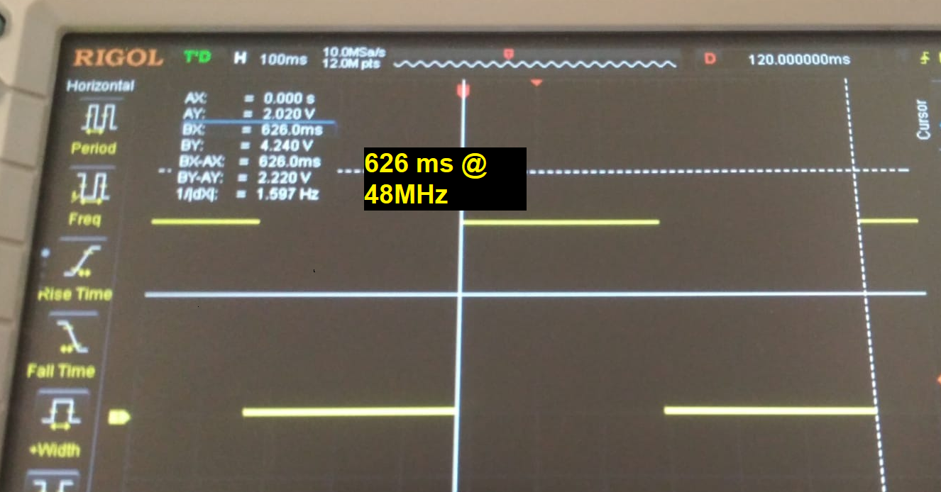
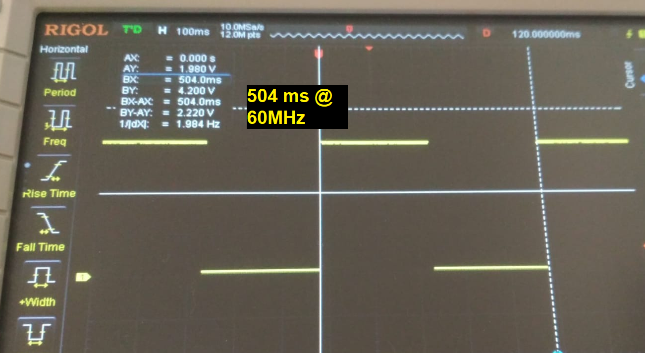
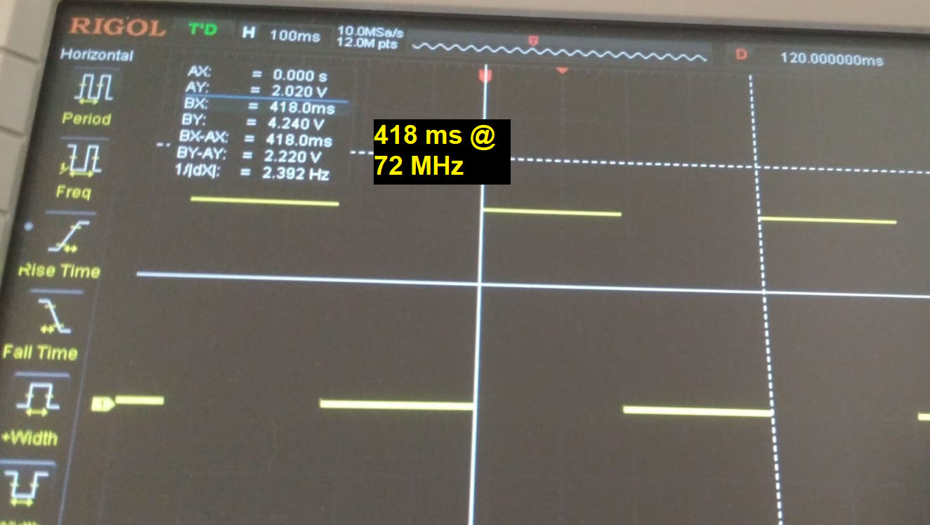
In any case, with our simple test code, we did not find any speed difference between code in RAM and flash memory. This is due to the very small code, that reasonably well fits the 64-byte cache. The results are:
@ 48 MHz: 626 ms.
@ 60 MHz: 504 ms.
@ 72 MHz: 418 ms.
We also verified that the device still runs very cold, but we cannot guarantee that the code will always be reliably executed: use this hack at your own risk!
What about the current consumption?
The program with uChip at 48MHz running from flash consumes 7.7mA. At 60 MHz, we get 9.4mA. At 72 MHz we get 11.0mA. 70MHz: 10.6 mA.
From RAM we get:
@48MHz: 8.8mA
@60MHz: 10.6mA
@70MHz: 12.0 mA
Please note that these values are taken as the USB current consumption, using an USB power meter. The measured USB voltage was 5.14V.
Conclusion
We have managed to run our devices at 70MHz, i.e. about a 50% overclock, that’s not bad indeed! Still, you should understand that these devices could behave erratically especially if they work in high temperature environments. Indeed, we tested all our devices at room temperature (22°C).
What speed
did you get? Write in the comments!
Downloads
[1] When working as USB device, the ATSAMD21 can also use the USB start of frame as reference frequency, which occurs once per millisecond, with a good precision.
[2] Note! This is just the AVERAGE number! Of course the number of wait states for each instruction will be always an integer!
Wow thats a cool idear to give the older Arduino Zero boards more speed if needed…
Would still be cool if the ide offered some “profile” selection for the board for automatic overclocking, what this is essentially with differen clock profile.
I do use the “ATSAMD21” based boards a lot for experiments where the classic uno is way too slow, the esp8266 has not enought i/o ports and feels like a hakery board from china :-/
Thank you for this highly informative article i liked it