
Many times we must interface 5V to 3.3V devices. This occurs very frequently on Arduino, but also other applications may need 5V to 3.3V ICs or systems to communicate. In many cases, some sort of logic level shifter/translation/conversion circuitry might be necessary.
For instance, imagine you want to connect to your Arduino Uno, which works at 5V, a 3.3V device, such as the display we used in our guide “How to play a video on Arduino Uno (2/6)”. Similarly, there are many 5V devices or shields, that cannot be used with an Arduino 2 or Zero, which works at 3.3 V.
In this post, we will talk about 5V to 3.3V logic level interfacing. For the opposite task, i.e. 3.3V to 5V conversion, see this article.
There are many ways to interface a 5V output to 3.3V input. The most common are:
- Direct Connection (Warning: Only With 5V Tolerant Inputs!!!)
- Series resistor.
- Series resistor with external Schottky diode clamp toward the 3.3V line.
- Series diode with pull-up resistor.
- Series resistor with active clamp.
- Resistor and Zener diode.
- Resistor divider.
- BJT/MOSFET as inverters.
- Two cascaded BJT/MOSFET as buffer.
- Pull-up resistor on open drain/collector outputs.
- Adding 5V-powered logic ICs (buffer, gates, etc) with open drain/collector output.
- Adding 3.3V-powered logic ics (buffer, gates, etc) with 5-V tolerant input.
- Series MOSFET (common gate configuration).
- Series BJT (common base configuration).
- Level translator.
- Optocoupler.
Note! In the following figures, all the resistors have the “R” label inside the symbol. This does not mean that the resistor shall have all the same value!
DIRECT CONNECTION (WARNING: ONLY WITH 5V TOLERANT INPUTS!!!)
The simplest way is, a direct connection. This is the case of the Arduino Ethernet Shield: the Wiznet W5500 Ethernet chip works at 3.3V but has 5V tolerant Inputs (see datasheet). The Arduino 2, instead, has NO 5V tolerant input, therefore you should never directly connect a 5V output to any of its input pins!
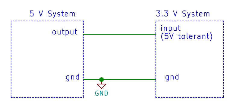
Fig. 1. Direct connection is possible if the 3.3V device has a 5-V tolerant input.
Advantages:
- No additional cost or space.
- Fastest solution.
Disadvantages:
- It works only on 5V-tolerant devices.
SERIES RESISTOR
The second simplest way to interface a 5V to a 3.3V system is to use a series resistor.
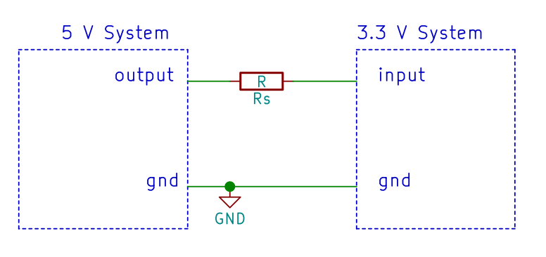
Fig. 2. Series resistor used to interface a 5V output to a 3.3V input. The input must have its protection diodes!
How does it work:
The input of a 3.3V (non 5V tolerant IC) is normally protected by diodes: one is toward VDD, another is toward GND, as shown in the figure below.These diodes are normally OFF as they are both reverse biased. However, if you try to put a voltage larger than VDD,3.3V, they will clamp the input voltage to VDD,3.3V (plus the forward diode voltage, normally 0.7V). Transient spikes larger than VDD,3.3V can occur even on a 3.3V-only system, due to capacitive coupling of switching device, or ringing.
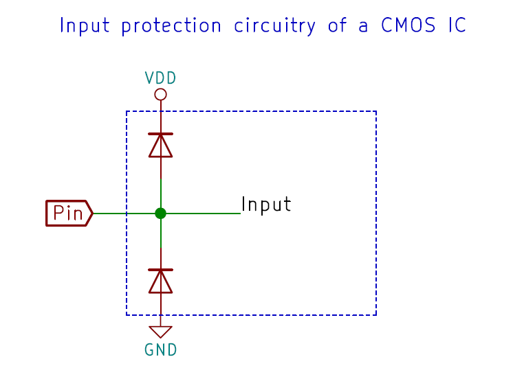
Fig. 3. Simplified schematics of the input protection circuitry on a CMOS IC.
When a 5V is fed through the resistor to the input, the diode will turn on: the resistor limits the current that flows into the pin, protecting the input. The maximum current into pin is sometimes indicated in the datasheet, and it should be kept low for two reasons:
- Normally, except the leakage current, no current would flow into a pin. Damage could occur, due to latch-up phenomena.
- The current flowing into the input pin, will flow OUT from the VDD pins! If such current is too large, it could increase the VDD voltage of the whole system, destroying the IC. If the system has a current consumption which is larger than the current flowing into the PIN, then there should be no problems. Otherwise, it’s advisable to put a dummy load, between VDD,3.3V and GND. The value of the load should be so that it adsorbs at least the current flowing into ALL The inputs.
To calculate this, simply consider the input current as I=(5V-3.3V)/RS. Then put between VDD,3.3V and GND a resistor such that it will draw the same current I. In other words: RLOAD = RS 3.3V (5V-3.3V) or about 2 RS. If you have more than one input, RLOAD must be decreased accordingly. If your system already draws “I” from the 3.3V (e.g. due to the IC current consumption, or presence of an always-on LED), then you might omit or increase RLOAD.
This solution has also another drawback: it severely limits the bandwidth, unless low valued resistors are used. In fact, the input pin and the traces will have a certain parasitic capacitance Cparasitic.
The bandwidth of the system is fC=1/(2πRSCparasitic). This does not means that you can hope for a fC digital clock signal to pass without being severely distorted. Here we plot a 500kHz square wave, after a filter, with a 1-MHz fC.
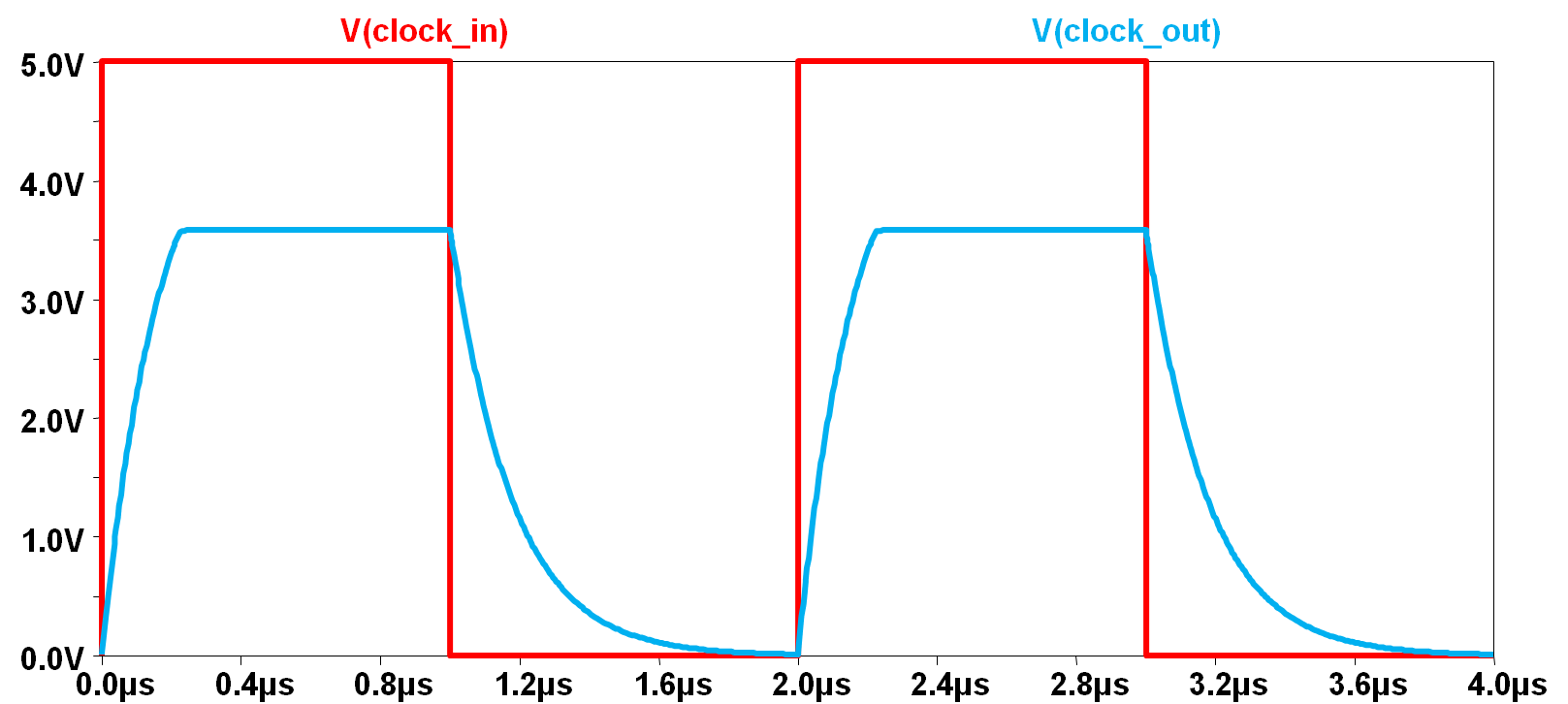
Fig. 4. A 500-kHz clock is fed to the circuit of Fig.2 (red line). The blue line is the actual obtained waveform.
To improve the bandwidth, low-value resistors should be used. However, low value resistors are not advisable for these reasons:
- The already mentioned current into pin.
- The current consumption.
- The overload of the output.
- It generates additional noises on the VDD,3.3V line as the input is switched.
Practical values are in the 1-10kOhm.
Advantages:
- Simple solution: just one resistor per input pin.
Disadvantages:
- High power usage (with low-value resistors) or poor bandwidth (high value resistors).
- Output overload (with low-value resistors)
- The current going into the input might cause latch up.
- Requires an external load resistors on the 3.3V supply, if the 3.3V system has a very low minimum current consumption.
- Possible noise on the 3.3V supply due to current injected into it.
- The 3.3V input must have a high impedance (small input leakage, such as CMOS).
SERIES RESISTOR WITH EXTERNAL SCHOTTKY DIODE CLAMP TOWARD THE 3.3V LINE.
This circuit is similar to the previous solution, however faster speeds can be achieved, because the majority of the current will be carried by the schottky diode, instead of the protection diodes.
This still has the drawback of having the current being fed to the VDD,3.3V line. Such current must therefore be “consumed” by the system, as shown for the previous case.
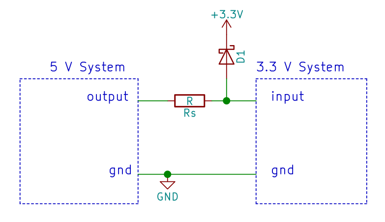
Fig. 5. Adding a Schottky diode, allows using smaller resistors, thus improving the bandwidth.
Advantages:
- Larger bandwidth achievable.
- Negligible current injected into input pin.
Disadvantages:
- Requires two components per input (resistor and Schottky diode).
- High power usage (with low-value resistors) or poor bandwidth (high value resistors).
- Output overload (with low-value resistors)
- Requires an external load resistors on the 3.3V supply, if the 3.3V system has a very low minimum current consumption.
- Possible noise on the 3.3V supply due to current injected into it.
- The capacitance of the diode must be still taken into account.
- The 3.3V input must have a high impedance (small input leakage, such as CMOS).
SERIES RESISTOR WITH ACTIVE CLAMP.
Instead of redirecting the input current toward VDD,3.3V, it’s better to dissipate it to ground, so no VDD,3.3V level variations will occur.
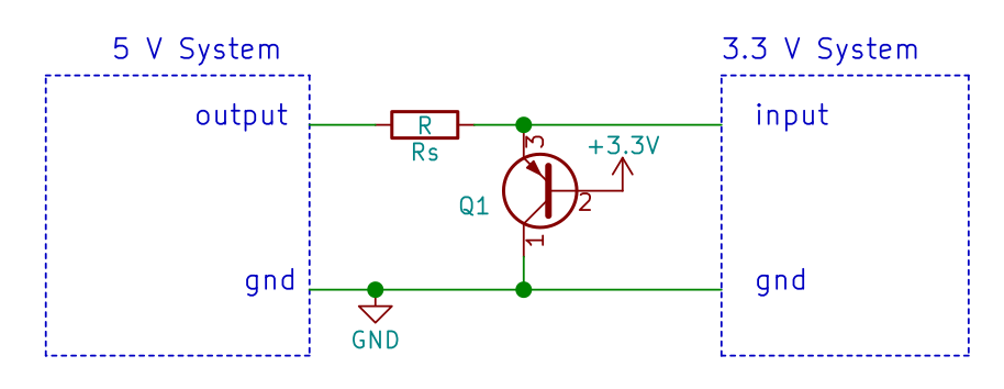
Fig. 6. A PNP BJT can be used as active clamp, by shorting to ground (instead of 3.3V) the excess current.
The PNP BJT will conduct as long when the input voltage is larger than 3.9V.
This solution allows using smaller resistors (higher bandwidth).
Noticeably, there will be still current injected into the VDD,3.3V, however, such current will be hFE times smaller than the current flowing into the RS. Therefore, in the majority of the cases, no RLOAD is required.
Another problem is that, on some ICs, their protection diode start conducting when the values on the input is as low as 0.35V above the 3.3V level. In such case, the BJT base should not be tied to 3.3V, but to a somewhat smaller voltage, if available on the system.
Advantages:
- Even larger bandwidth achievable.
- Very small current injected into the 3.3V supply line.
- Small current injected into the input pin.
Disadvantages:
- Requires two components per input (resistor and BJT).
- High power usage (with low-value resistors) or poor bandwidth (high value resistors).
- Output overload (with low-value resistors)
- Still might require an external load resistors on the 3.3V supply, if the 3.3V system has an extremely low minimum current consumption.
- Still possible noise on the 3.3V supply due to current injected into it.
- In some cases, another supply (lower than 3.3V) could be required to clamp the voltage below the turn-on voltage of the input protection diodes.
- The capacitance of the BJT must be still taken into account.
- The 3.3V input must have a high impedance (small input leakage, such as CMOS).
- The clamping voltage might be too high (about 3.9V). Another voltage source (smaller than 3.3V) could be required.
RESISTOR AND ZENER DIODE
Instead of using a BJT, we can use a Zener diode, which will clip the voltage to the Vz value. The problem is that low valued Zener have a quite large dynamic resistance, and a large current must flow into the Zener, to actually exhibit the Vz value (several mA).
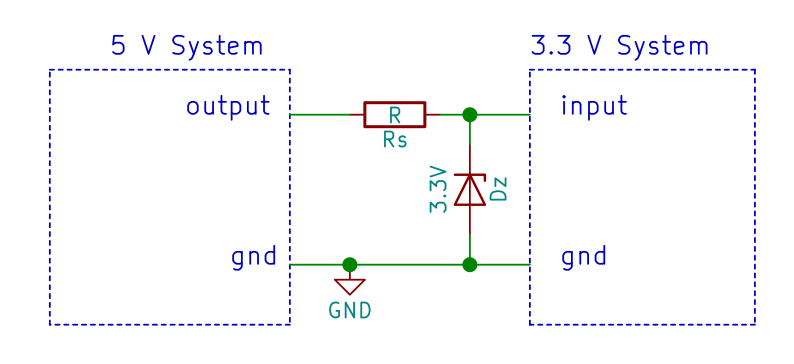
Fig. 7. A 3.3V Zener diode allows clamping the voltage.
Advantages:
- Bandwidth similar to the Schottky or active clamp solution, due to the possibility of using low-value resistors.
- No current injected into the 3.3V supply line.
- No current injected into input pin.
- Lower cost than the BJT or Schottky.
- The clamping voltage can be lower than the BJT.
Disadvantages:
- Requires two components per input (resistor and zener).
- High power usage (with low-value resistors) or poor bandwidth (high value resistors).
- Output overload (with low-value resistors)
- The capacitance of the diode must be still taken into account.
- The output voltage is not precise, because some low-valued Zener diodes have a very poor dynamic resistance.
- The 3.3V input must have a high impedance (small input leakage, such as CMOS).
SERIES DIODE WITH PULL-UP RESISTOR.
If your 3.3V system accept low-level input voltages as high as 0.7V, you can use a normal 1N4148 diode, as shown below. If you want more noise margin (or if simply 0.7V is too high), use a Schottky diode instead.
The working principle is simple: when the 5V system outputs 5V, the diode is reverse polarized, therefore it is open. The input of the 3.3V system is pulled up to 3.3V through R1. Then the 5V-system outputs 0V, the diode is forward biased, so the voltage at the 3.3V input will be the forward voltage drop of the diode: about 0.6-0.7V for silicon diodes, or 0.35V for Schottky diodes. Remember to use a fast signal diode! (i.e. do not use a 1N4007!).
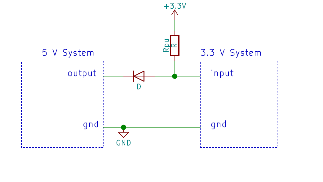
Fig. 8. A series switching diode (such as 1N4148) blocks the high level voltage. The series resistor pulls-up the output.
Advantages:
- Bandwidth similar to the Schottky clamp solution, due to the possibility of using low-value pull-up resistors.
- No current injected into the 3.3V supply line.
- No current injected into input pin.
Disadvantages:
- Requires two components per input (resistor and diode).
- High power usage (with low-value resistors) or poor bandwidth (high value resistors).
- Output overload (with low-value resistors)
- The capacitance of the diode must be still taken into account.
- The low-level output voltage is the forward voltage drop of the diode.
- The 3.3V input must have a high impedance (small input leakage, such as CMOS).
RESISTOR DIVIDER
One simple way to reduce the 5V voltage, is through a resistor divider!
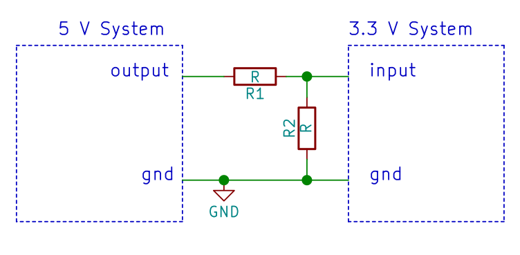
Fig. 9. A resistor divider.
The resistor divider performs a better job, with respect the single resistor. Given the same bandwidth, it consumes less with respect to the other solutions already examinated (except the direct connections!).
In fact, the bandwidth in all the solutions is determined by the time constant RSCparasitic (note also that the BJT or the diodes increase Cparasitic!!!). The current is (5V-3.3V)/RS. On the resistor divider, the current is (5V-3.3V)/R1. However, the bandwidth of the divider is determined by the time constant (R1//R2 Cparasitic). In other words, if RS=R1, the bandwidth will be higher on the divider. Conversely, if the bandwidth is the same, the current will be smaller.
The parasitic capacity of R2 still impact on the bandwidth, but this is much less with respect to a diode or a BJT.
Advantages:
- Better bandwidth with respect to the other systems (except direct connection) at the same consumption (or smaller consumption at the same bandwidth).
- No current injected into the 3.3V supply line.
- No current injected into input pin.
- Lower cost than the BJT, Schottky, or zener.
- Symmetric rise/fall times.
Disadvantages:
- Requires two components per input (two resistors).
- High power usage (with low-value resistors) or poor bandwidth (high value resistor).
- Output overload (with low-value resistors)
- The 3.3V input must have a high impedance (small input leakage, such as CMOS).
BJT/MOSFET AS INVERTERS
If you can live with inverted signals, you can use a BJT or MOSFET.
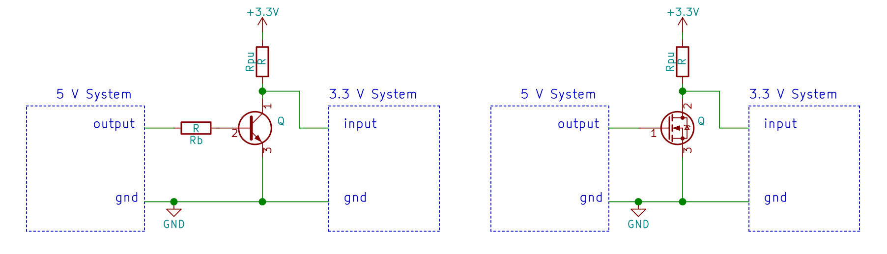
Fig. 10. A BJT/MOSFET as inverter can be used as level shifter.
The bandwidth is determined mainly by the pull-up resistor and the parasitic capacitance (which must include the capacitance of the BJT/MOSFET!).
Advantages:
- No current injected into the 3.3V supply line.
- No output overload.
- No current injected into input pin.
Disadvantages:
- Requires two or three components per input (the BJT/MOSFET and one or two resistors).
- High power usage (with low-value pull-up resistors)
- Inverted output!
- The 3.3V input must have a high impedance (small input leakage, such as CMOS).
TWO CASCADED BJT/MOSFET AS BUFFER.
You can cascade two of the previous BJT/MOSFET-resistor inverters. In this way the output is not inverted.
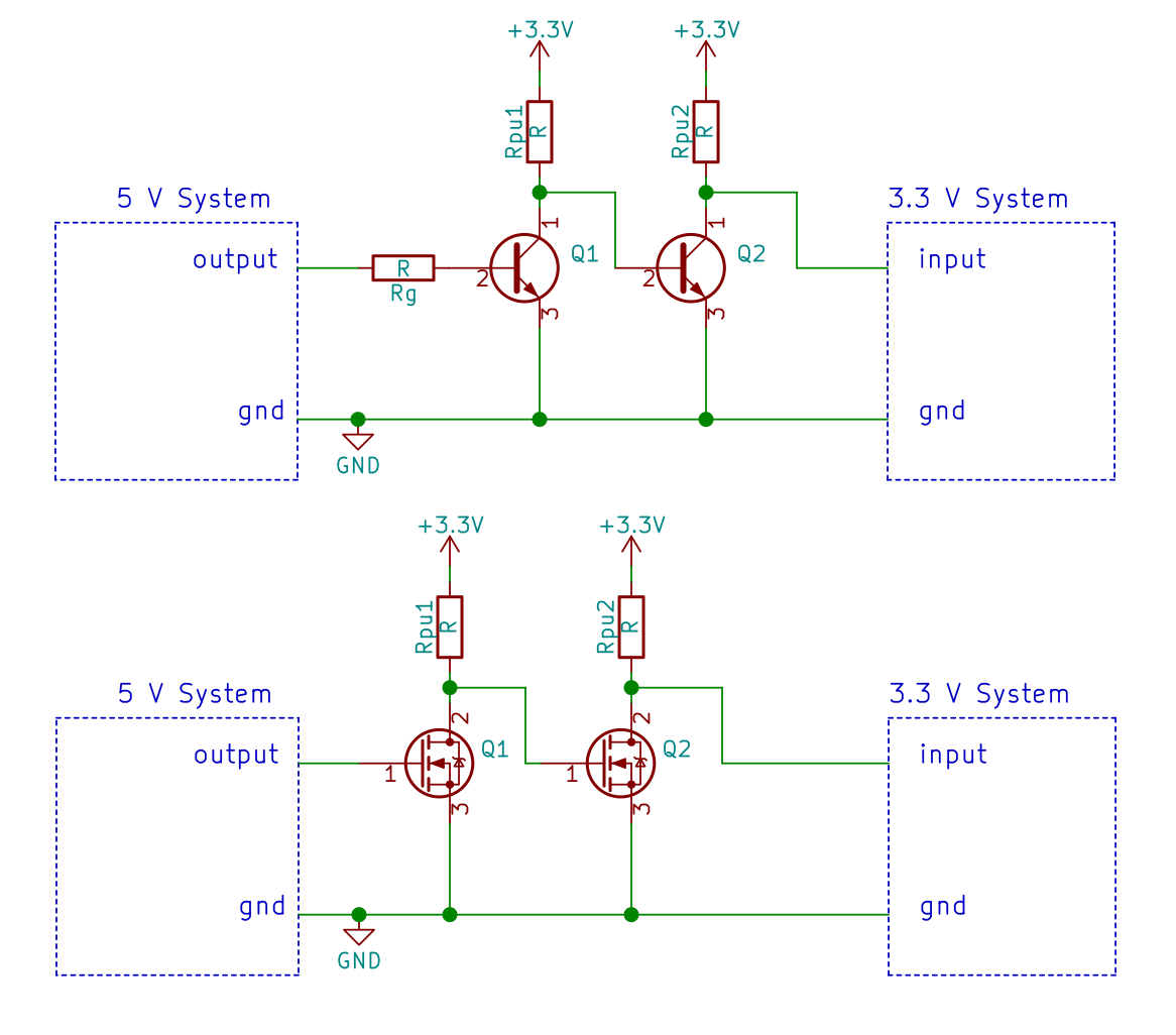
Fig. 11. You can cascade two inverters made with a BJT or MOSFET and achieve a level shifter.
Advantages:
- No current injected into the 3.3V supply line.
- No output overload.
- No current injected into input pin.
- The logic level is not inverted.
Disadvantages:
- Requires a lot of components!
- High power usage (with low-value pull-up resistors)
- The 3.3V input must have a high impedance (small input leakage, such as CMOS).
- Bandwidth smaller with respect to the previous case, because of the cascading of two stages.
PULL-UP RESISTOR on OPEN DRAIN/COLLECOR OUTPUTs.
This WORKS ONLY if the output is an open collector/drain
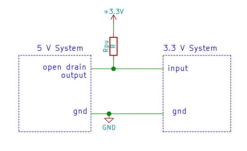
Fig. 12. If the output is a open drain/collector, you can use a pull-up resistor.
This is extremely similar to the “BJT/MOSFET as inverter”. Since the output is open drain, a pull-up resistor must be inserted.
Advantages:
- Single resistor required.
- No current injected into pin.
- No current injected into the 3.3V line.
Disadvantages:
- High power usage (with low-value resistors) or poor bandwidth (high value resistors).
- The 3.3V input must have a high impedance (small input leakage, such as CMOS).
LOGIC ICs (Buffer, gates, etc) WITH OPEN DRAIN/COLLECTOR OUTPUT.
You can connect open drain/collector buffer/gate IC, plus a pull up resistor as shown below. The buffer/gate is powered with the 5V, so that it will accept the 5V.
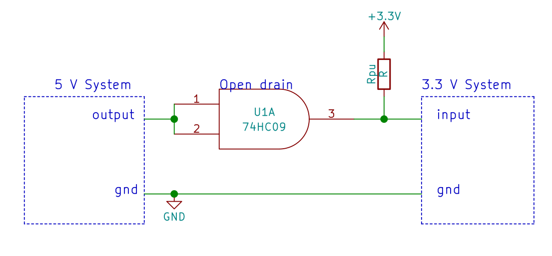
Fig. 13. You can add a gate (e.g. 74HC09) or a buffer (e.g. 74LS07) powered at 5V, with an open drain output.
Advantages:
- No current injected into pin.
- No current injected into the 3.3V line.
Disadvantages:
- High power usage (with low-value resistors) or poor bandwidth (high value resistors).
- This solution requires a buffer and a resistor.
- The 3.3V input must have a high impedance (small input leakage, such as CMOS).
ADDING 3.3V-POWERED LOGIC ICs (Buffer, gates, etc) WITH 5-V tolerant input.
You can connect a 5V tolerant IC, powered at 3.3V, such as SN74LV1T34.
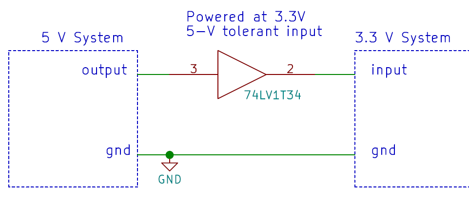
Fig. 14. You can add a 5-V tolerant buffer (powered at 3.3V).
Advantages:
- No current injected into pin.
- No current injected into the 3.3V line.
- Low power.
- Fast.
- High noise margin.
Disadvantages:
- Cost and space
SERIES MOSFET (common gate configuration)
Instead of using the MOSFET in common source configuration, we can use the commong gate configuration. The MOSFET will be actually in series. The MOSFET must be a 2.5V logic level MOSFET otherwise it won’t work.
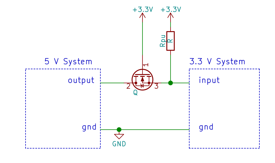
Fig. 15. A series MOSFET can be used as translator.
The circuit works as follows.
When the VIN is at 5V, the MOSFET will be OFF, as VGS = 0V (tied up by R2). When VIN is 0V, the output will initially go to 0.7V, due to the drain-body parasitic diode of the MOSFET. Therefore VGS will become 3.3V-0.7V = 2.6V. Since this is a 2.5-V logic level MOSFET, the MOSFET will turn on, effectively acting now as a short. The output will be 0V.
As we will show in “Interfacing a 3.3V to 5V system”, this circuit works also bidirectionally, i.e. it translates a 3.3V signal into a 5V signal!
Advantages:
- No current injected into the 3.3V supply line.
- No current injected into input pin.
- Non-inverted output.
- Can be bidirectional.
Disadvantages:
- Requires two components per input (the MOSFET and one resistor).
- High power usage (with low-value pull-up resistors)
- Output overload (with low-value pull-up resistors)
- The capacitance of the MOSFET must be still taken into account.
- Requires a 2.5V logic level MOSFET.
- The 3.3V input must have a high impedance (small input leakage, such as CMOS).
SERIES BJT (common base configuration)
A BJT can be also used, however the emitter must be on the 5V side (the source of the MOSFET was, instead, on the 3.3V side!).
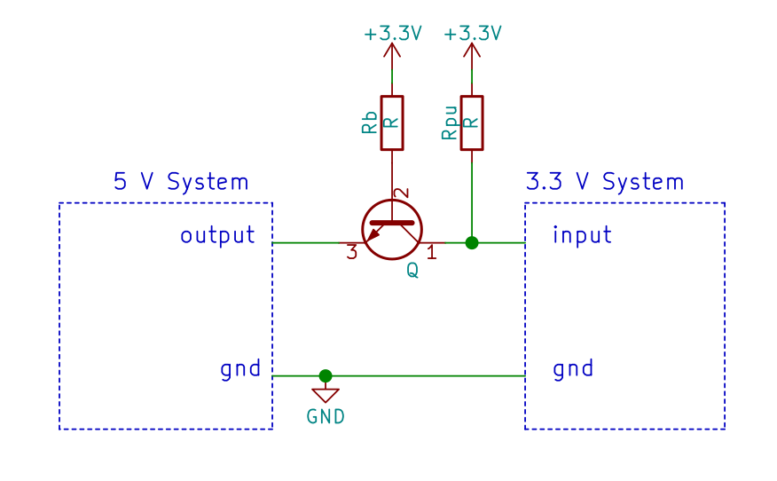
Fig. 16. The BJT can be used as series translator as well!
It works as follows: when the input is 5V, VBE=-1.7, therefore the BJT is OFF. The 3.3V side is pulled-up. When the VIN is 0V, the base-emitter junction will be forward polarized, and the BJT will turn on, transmitting the “0” logic level to the 3.3V side.
Advantages:
- No current injected into the 3.3V supply line.
- No current injected into input pin.
- Non inverted output.
Disadvantages:
- Requires three components per input (the BJT and two resistors).
- High power usage (with low-value pull-up resistors)
- Output overload (with low-value pull-up resistors)
- The capacitance of the BJT must be still taken into account.
- VCE,sat is added to the low value output.
- The 3.3V input must have a high impedance (small input leakage, such as CMOS).
LEVEL TRANSLATOR
To achieve the fastest speed, lowest power consumption and better signal levels, you can use a level translator IC such as 74LVC8T245 (8 bit) or 74LVC1T45 (1 bit). They however cost a lot, occupy space, and require other two decoupling capacitors (not shown in the schematics).
Usually level translators come with different number of inputs/outputs, they can be also bidirectional (either controlled by data direction, or automatic).
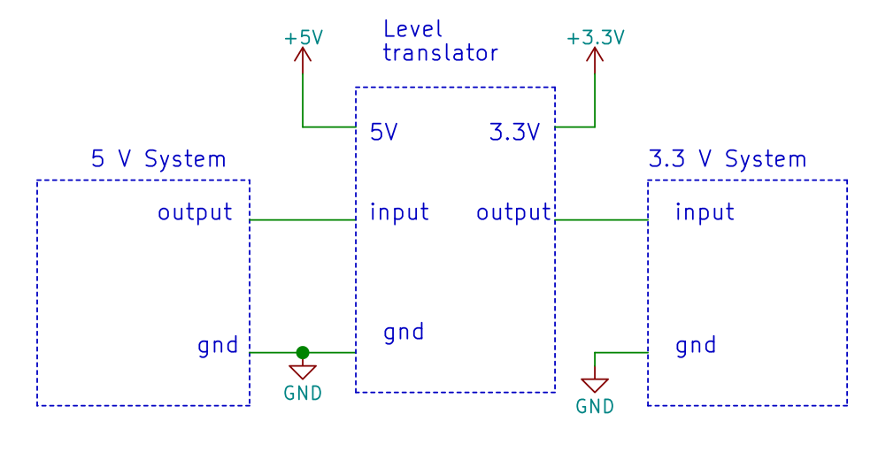
Fig. 17. A level translator allows for the cleanest signal, with the best performance. However, it adds space and cost.
Advantages:
- No current injected into the 3.3V supply line.
- No current injected into input pin.
- Not inverted output (There are also inverting translators too).
- No output overload.
- Very high bandwidth.
- Good signal levels.
- The output of the transceiver can be also loaded.
- Negligible static power consumption.
Disadvantages:
- Cost (level translators are much more expensive than a pair of resistors or a MOSFET/diode).
- Space required (especially with if few inputs are required).
OPTOCOUPLER/ISOLATOR
This technique is especially useful and recommended when you need to interface two separate systems, or when you need electrical insulation between two parts of the same circuit/system. It is also very useful when dealing with voltages much higher than 5V (e.g. 24V).
Note that the two systems might share the same ground too, but, in this case you will lose the electrical insulation between them.
There are 4 variants, considering the inverting or non inverting configuration.
In the schematics below, we show a standard optocoupler, with a transistor output. There are optocouplers that already provide a digital, and, wtih them, in some cases Rpu is not needed (check if the output is open collector).
Recently, other kinds of isolators have been available. These are not optical based, but rather on capacitive, giant magnetoresistive or magnetic couplings. These are generally faster, but much more expensive.
In all these optocoupler/isolator, with a direct digital output, only the first version of both the inverting and non inverting configurations can be used (i.e. where the optocoupler is connected between the input of the 3.3V system and ground).
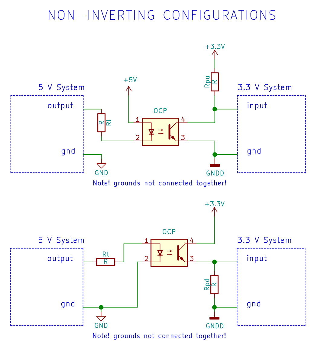
Fig. 18. Two non inverting configurations using an optocoupler. Note that if the optocoupler has a digital output, such as TLP2710 (and not a phototransistor output as shown in the schematics), then the correct non-inverting configuration is the first one. In such case, you must also connect the VDD and you don’t need Rpu. If the optocoupler has a digital output but it is open collector (such as TLP2719), Rpu is required.
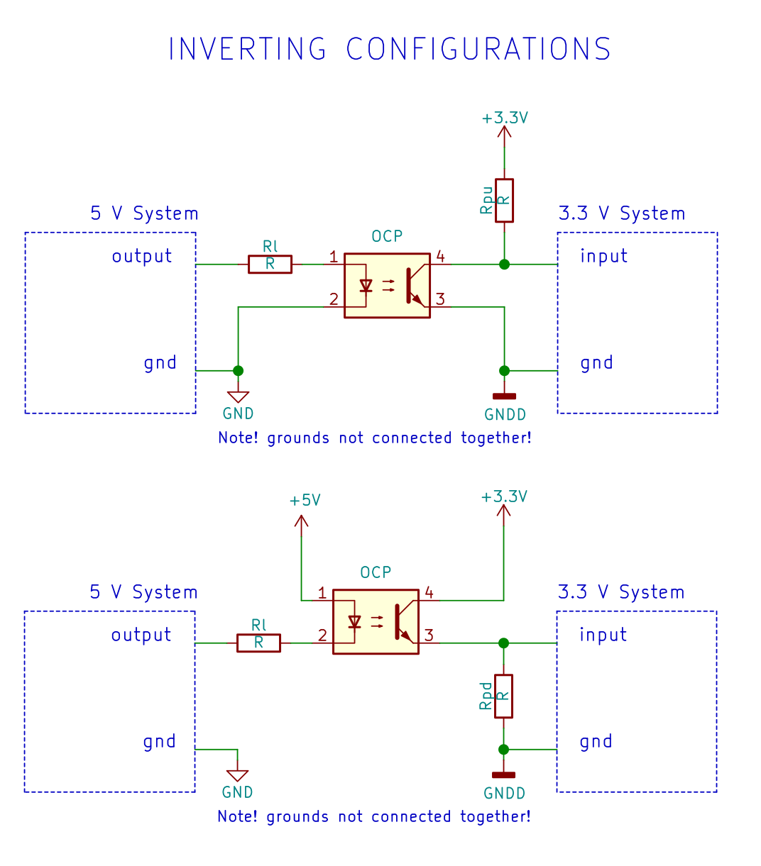
Fig. 19. Two inverting configurations using an optocoupler. Note that if the optocoupler has a digital output, such as TLP2710 (and not a phototransistor output as shown in the schematics), then the correct inverting configuration is the first one. In such case, you must also connect the VDD and you don’t need Rpu. If the optocoupler has a digital output but it is open collector (such as TLP2719), Rpu is required.
Advantages:
- Electrical insulation between the two system. Not only it provides better noise performance, but also increases the safety of the system.
- Allows to convert any voltage level to “any” voltage level.
- By properly choosing the ground or power supply (depending on the configuration), you can achieve other kinds of voltage translation (e.g. -12V…+12V to 0…3.3V translation).
Disadvantages:
- It requires an optocoupler.
- Standard optocouplers are typically slow. For high data rates, special “high-speed” optocouplers are required.
- Relatively high current consumption due to the internal LED.
- The power consumption is higher if high bandwidth is required, as Rpu/Rpd need to be rather small, if small rise/fall times are required.
Conclusions
These are just some of the many possibilities.
We will be adding them as soon as they come into our mind :).
If you need instead to interface a 3.3V output to a 5V input, click here!
Liked the article giving many good practical approached. But I fail to understand why a simple 3V3 voltage regulator cannot/ is not used. I must be missing something.
Do help me out pse.
Hi Alan!
We are glad you liked the post.
A 3.3V voltage regulator is used to provide the power supply for the 3.3V chips, such as logic ICs, microcontrollers, analog stuff etc. However, it cannot be used* to convert a 5V binary signal, which can be 5V or 0V, to a 3.3V one.
*well, in principle one could use a linear regulator to convert a 5V digital signal – provided that the 5V logic output can source enough current – to a 3V3 one**. However this would be a very inefficient and expensive way. For instance many regulator are simply too slow, or they can oscillate in absence of input and output capacitors. Such capacitors would further impact the speed – down to some kHz- and the dynamic power consumption. At this point a single high valued resistor would provide a much better solution.
** you would still require a rather low valued pull down resistor, to create a 0 logic level. This is because most of the linear regulator simply consist of a series PNP (LDO) or NPN transistor, so there is “almost nothing” (expect the resistor divider feedback network, which might be extremely high in low power devices) to “pull down” the output.
Dang. I thought I was good. Quite the list of tricks. Props.
Excellent page, It is quite difficult to find comprehensive Discrete circuit comparison on the web like this.. Seems that some of the simplier solutions are even better than the most evolved ones (With FET/BJT). Maybe something to highligh
Can you suggest one of these circuits (or another one) to interface ANY voltage in the region of 5V to 24V? (I mean, 5-24V must be translated to 3.3V and 0V to 0V).
Hi Vassilis, we suggest in this case an optocoupler! We will add the corresponding circuit shortly!
Hi. This excellent article (and the companion one) are a few years old, so I hope you are still responding to comments and questions.
In the series BJT configurations (this page’s Figure 16, and the companion article page’s Figure 13) you show the collector (pull-up) resistor and the base resistor, as both having a value of “R”. Does this mean that both resistors should actually be the same value? (I realise that, when “switched on”, the BJT is in saturation mode, so the base current only needs to be enough to drive the BJT into saturation – i.e. the actual resistor values are not terribly critical, so long as the BJT goes into saturation).
I want to use an Arduino UNO (using an ATmega328P processor, running at 5V) to develop, test and FLASH program, a project using a PIC12LF1840 micro. Since the PIC device is a LF (i.e. Microchip “XLP”) device, it must have a supply of 3.6V or lower. So, during development, I plan to use the Arduino UNO’s 3.3V power output, to power the PIC device and related circuitry (which are all very low power, so the UNO 3.3V supply current should be plenty for this.) However, the UNO”s I/O pins are, of course 5V logic signals.
So, for development and testing, I think that using the non-inverting, series BJT configurations (in both directions), between the UNO and the PIC device, is the way to go, since I have a handful of 2N3904 BJTs available.
My question is, what would be “good” values to use for the base and collector resistors? For development, power is ultimately supplied from PC USB port, so power consumption is not a concern (other than to ensure current limit specs on the UNO and PIC device I/O pins, and the UNO’s 3.3V power supply output).
Thanks and very best regards,
Ed.
Hi Ed, thank you for the compliments and reading the article. Actually R is a placeholder for the resistor value, and the fact that both resistors have R inside does not mean the values must be the same. I realize this might be confusing, and I am adding a note in the article right now.
Regarding values: the most important resistor is the pull-up on the right side. The smaller, the faster low-to-high transition. How fast are you going? Depending on the frequency, values around 2.2k -4.7k might be good. Next is the base resistor value. It shall bring the BJT to saturation, but remember that a strongly saturted BJT has a slow turn-off time. In practice we expect that a 47k value might work well with your 3904s.
And my second question is like unto the first. : )
Once development is complete, the PIC12LF1840 micro will be powered at 3V using two AA cells in series. One of the inputs to the PIC micro, is an accurate time base from a cheap 1.5V electronic “module” extracted from a quartz wall-clock motor. The Lavet stepper-motor coil will be removed from the electronic module, and one of module’s two outputs will supply a short 1.5V pulse (about 20 – 50 ms width – I have not measured it yet) exactly once every 2 seconds. (These things are super accurate; think of how often you need to correct the time on one of these wall clocks! Almost never, right? Well, except, of course, when the battery gets low, or the time changes between standard and daylight-savings. 😉
So, the pulse train output from the wall clock electronic module consists of +1.5V pulses, with a pulse width of about 35 mS (+/- 15 ms, or so), and has a period of exactly 2 seconds. This will be delivered to the interrupt input of the PIC12LF1840, using as little power as possible, since these are running off of batteries. The PIC12LF1840 will normally be in sleep mode, and each pulse from the clock module will generate a wake-up interrupt (every 2 seconds), triggering a very short processing routine in the PIC device, before it goes back to sleep. BTW, it does not matter if the pulses from the clock module are inverted, or not, when delivered to the PIC12LF1840 input. The whole thing will be powered off of two AA cells, to supply nominal 3V to the PIC12LF1840, and a “center tap” supplying 1.5V to the clock module. Ideally, I would like the batteries to last as long as would a single battery that normally powers a quartz wall-clock.
So, now to my shifty level-shifting questions:
1. Again, since I have a handful of 2N3904 BJT’s available, I am thinking of either: a) the inverting, common emitter configuration (something like the BJT version in Figure 10 of this page, but the left side is a “1.5V System” and the right side is a “3V System”); OR b) the Series BJT configuration (something like Figure 16 of this page but, again, left side is 1.5V and right side is 3V). Which of these configurations should consume less power from the batteries?
2. In the “better” configuration chosen from question 1 above, what would be “good” resistor values for the base and collector resistors, to allow for least power consumption, but still perform well, overall? (I guess I am asking what the maximum collector and base resistances can be, and still perform well.)
Thanks and best regards,
Ed.
Hi again 🙂
If I have understood correctly, you want to connect the 1.5V 2-second pulse coming from the quartz clock circuitry to the 3-V PIC. Therefore the input is the 3V PIC and the output is the 1.5V signal. In this case, you should check the article https://next-hack.com/index.php/2020/02/15/how-to-interface-a-3-3v-output-to-a-5v-input/. (Yes, series and inverter configuration are present there too!).
On these configurations, consumption comes when the BJT is ON. I.e. in the common emitter, when the “high-voltage side” output is high, or in the series configuration, when the “high-voltage” side is low.
Since the input of the micro is very high impedance, and since the frequency is very low, then the pull up resistor value can be quite high, even 10k or 47k. If the micro has an internal pull-up resistor on its input (typically on many MCUs it is in the 10-50k range), you can use it, and remove the right-side pull-up resistor. A high pull-up value means a very small collector current flowing when the BJT is ON. About the base resistor value, since the pull-up resistor value is very high, then the base resistor value can be in the hundreds of kOhm range. I recommend however not to exaggerate too much with the resistor value, as the device might become too much sensitive to electrical noise, occasionally generating false triggers.
Thanks for this excellent article! Could you also write tips for 5V to 3.3V analog conversion? I am struggling in using voltage divider or opamp.
Thank you
Hi Gordon,
we will sooner or later make some articles on analog conversion!
Cheers!
I would use a 74LVC1g57 or other LVC single gate, they are very fast, only a few cents cents and come in small packages.
This is for isolating a noisy 5v transceiver from a quiet 3.3v analog section which has a LVDO regulator. I think that is a pretty common scenario.
Hi Robert!
These ICs are very nice, they can also implement different logic functions as well. However these still fall in the category “Adding 3.3V-powered logic ics (buffer, gates, etc) with 5-V tolerant input”, already described.
I want to use an IC 74HC4050-Q100 to tranfer the output my encoder(sendix: 50000) which has RS 422 TTL output circuit. It takes 5V dc as supply. HIGH: 2.5V(min) LOW: 0.5V (max).
Would that fall “Adding 3.3V-powered logic ics (buffer, gates, etc) with 5-V tolerant input” ?
If not, How does one connect 4 inputs and outputs of this IC?
I only have two output from encoder to read, A and B. It would be very helpful, if anyone can explain interfacing this IC to me.
Sorry I had to edit my comment:
I want to use an IC 74HC4050-Q100 to transfer the output of my encoder to Rasberry PI PICO(takes 3.3V input) (sendix: 50000) which has RS 422 TTL output circuit. It takes 5V dc as supply. HIGH: 2.5V(min) LOW: 0.5V (max).
Hi Faziay Rabbi! This is a 5V tolerant input IC, so you can use it. Simply connect 5V outputs to 74HC4050’s input. Remember to power 74HC4050 at 3.3V.
Outstanding article! I’ll be using “SERIES DIODE WITH PULL-UP RESISTOR” for my ESP8266 project. You saved me a lot of time and educated me, too. Thanks!
I would think the series diode and pullup is overall the best option for speed and current consumption, also cheap.
Particularly so for a signal that is mostly HIGH.
If mostly LOW, then the resistor divider is the lowest current consumption. Note that analysis of the bandwidth is rather tricky. The resistive component of “R*C” is the parallel resistance of the two, but the intrinsic capacitance of the resistors cancels and is small anyway.
Hello to all.
Thank you for this excellent article.
I’m pretty much a beginner and I’m implementing the Optocoupler based solution to interface an ESP32 (3.3v) with 5v devices.
In figure 18, Why does it say “In case of digital output, only the first choice is typically possible.” ? Is it true for active high and active low configurations ?
Thanks for your help.
Hi Damien, thank you, it was indeed misleading. We have reworded it differently. What we meant is that if the optocoupler has a digital output, then there is only one way to connect it.
What are the values in ohms of R1 and R2 for the “resistor divider” case?
It’s a tradeoff between speed and power consumption. For instance you might use 2.2k and 3.3 kOhm. Or 1 and 1.5 kOhm for higher speed.
Brilliant article – thank you very much.
I’m attempting to interface a 4-5v line signal to a 3v3 digital input (CMOS 2:1 mux, as it happens) and was planning on adopting something similar to the ‘BJT as Inverter’/Fig. 10 approach, with a Rb of 10k to reduce loading of the line signal.
The 3v3 input is already pulled-up with 1.5k (part of the input cct I can’t reach) and also has an ESD diode array to Gnd protecting it.
However, I have a question regarding the behaviour of the BJT with c. 5v at the base and only 3v3 (via that pull-up) at the collector.
Would this not upset the BJT having the collector-base V reverse-biased?
I don’t see an ‘absolute maximum’ specified for such a reversed biased base-collector on the datasheet for the BC546 I intended to use but my (possibly flawed) BJT understanding suggests reverse-biassing collector-base isn’t healthy?
Hoping to be re-educated – please don’t hold back!
Hi Martyn,
When the output driving the BJT is at 5V, the voltage at the base will be between 0.6-0.8V (the base-emitter junction being forward biased). The remaining 4.2-4.4V will drop on Rb.
Actually, in this configuration, the base-collector junction is (slightly) forward biased.
When using the BJT as analog amplifier (i.e. not this case!), the base-collector junction is always reverse biased, and you must not exceed the Vcbo reverse voltage specified in the datasheet. For the BC546, it is 80V (see https://www.onsemi.com/pdf/datasheet/bc546-d.pdf).
Cheers!
Insufficient information of course – you need to properly characterise your “4-5v line signal” and really, explain what it is and what is its purpose.
The advantage of the series diode with pullup is twofold, it does not matter what the input voltage is as long as it exceeds 3 Volts, and it does not matter if a signal is present but the 3.3 V system is not powered.
This significant concern was omitted in the original article.