
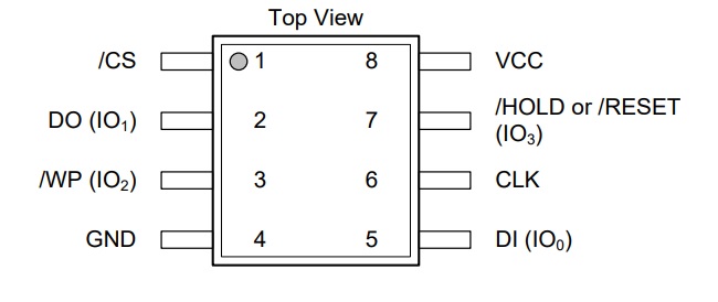
“… if it exists, it can run Doom.”
It’s again Doom time!
Time to add one more device to the list of unusual things that run Doom!
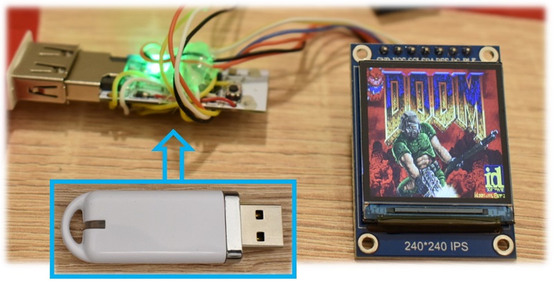
Now, as the title says, we will be targeting a $13 (excluding shipping) Bluetooth LE USB adapter.
This adapter is based on the nRF52840, an IoT RF microcontroller (MCU hereafter), by Nordic Semiconductors (Nordic hereafter).
The purposes of this project are:
- Port Doom to another device, which is not meant to play Doom at all.
- Port Doom to the nRF52840 MCU, i.e. to all devices based on the same microcontroller, provided they have enough accessible GPIOs, to add a QSPI memory, and a display.
- Show once again that some everyday-use low-cost devices are actually powerful enough to run Doom (even faster than you used to on 1993), despite their apparent simplicity.
The nRF52840 MCU
The nRF52840 features a 64 MHz Cortex M4 (CM4 hereafter), with 256 kB of RAM and 1 MB of flash.
In terms of computing power, this MCU is much less powerful than the 80-MHz Cortex M33 (CM33 hereafter) we used previously. In fact, considering the different DMIPS/MHz (1.25 vs 1.5) and the different clock (64 vs 80 MHz), the CM33 was 1.5 times faster.
However, unlike the CM33, this CM4 MCU features also a hardware QSPI interface, which also supports memory mapping, i.e. the flash memory can be read as if it was part of the microcontroller internal memory: the QSPI module will handle flash read command and address generation. The maximum QSPI clock speed is 32 MHz, allowing for a peak 16 MB/s transfer rate. Still, as we will see later, to get the maximum from the QSPI peripheral, we rarely access it in memory-mapped mode, especially for random read operations.
In terms of RAM, the nRF52840 has almost 2.5 times the RAM we had in the previous project (a quarter of MB, instead of less than a ninth). The now available much larger RAM allows us to use a much higher resolution display, without having to worry too much about the frame buffer. We can also implement double buffering, which, together with DMA, will provide a huge performance boost, as we can render a new frame, while the old one is being sent to the display.
Finally, we have 1 MB flash: same as we had before.
Previous Doom Port Attempts on the nRF52840
Before starting this project, someone pointed us to this blog post from a Nordic engineer, who ported Doom to the nRF5340, which is a more powerful MCU with respect to nRF52840. The article also points to a couple of videos that show the game in action. In the most recent video, the game is running very smoothly at 34-35 fps the majority of time, slowing down below the 30fps mark only occasionally, in complex areas. (35 fps is the software-enforced limit of the original Doom, and it has been kept in many ports. This is known as frame rate cap).
Still, the nRF5340 is an extremely powerful dual-core CM33 microcontroller: one core is clocked at 128 MHz and features 512kB of RAM + 1MB of flash, the other core runs at 64 MHz and has 256kB Flash and 64kB RAM. The microcontroller also features a 96MHz QSPI interface, i.e data can be read at 48 MB/s. From such high-end specs, in terms of DMIPS, RAM amount and QSPI speed, the achieved performance is quite expectable, even on a 320×200 display.
Then, it took us a single Google search to discover that the same employee also managed to “run” Doom on the nRF52840, as a proof of concept. However, by looking at their published video, the frame rate was very low. In fact, by counting the frames on the video, we estimate a 3 to 5 fps value on level E1M1. Furthermore, many textures, including the sky, were changed with a placeholder, probably due to memory and speed issues.

This is not surprising, since from the published video we see that the bare nRF52840 dev-board was used, with no external QSPI flash. Therefore, we assume that all the data was read directly from the SD card, which introduces quite a huge overhead, especially if a file system is used. This might explain why such low frame rate was achieved.
While this is “ok” for a proof of concept, the frame rate is not high enough for actual gameplay. This was also a good reason to start our adventure.
Despite this is not the first time Doom has been ported to the nRF52840, we wanted to tell our story. Can we do better with the same MCU? By how much?
The Challenge
We have already shown that with less than an ninth of MB of RAM you can run Doom, and we stated that the performance limiting factors were the small RAM amount and the access speed to graphics data, stored on an external serial flash. Now we have a quarter of MB, and a faster interface to the external flash, so we cannot keep our expectations low, even if this microcontroller has only 2/3 of the computing power we had previously.
Here are the rules:
- We want to be able to run the full commercial Doom, i.e. all the levels of the three original episodes should work at the ultra-violence mode. The only exception, for now, is multiplayer and music.
- An external QSPI flash can be added, to store the commercial WAD file.
- As already stated, the target device is a Bluetooth LE USB adapter. Of course, a Bluetooth dongle typically has no display, and we need to add one. Even if we have a less powerful microcontroller, we can take advantage of the more RAM for some speed optimizations, so we would like to increase the resolution, with respect to the past time, and bring it closer to the original Doom, at least in terms of number of 3D pixels, for a fair comparison (the resolution shall be higher than the default Doom viewport resolution, which is 288 x 144 pixels). We explain what we mean for “number of 3D pixels” in Appendix A, at the end of the article.
- All levels of all the three episode of the original Doom should be playable, with an average frame rate of 20 fps, at the ultra violence mode, despite the increased resolution. Spoiler: we admit we were too much pessimistic.
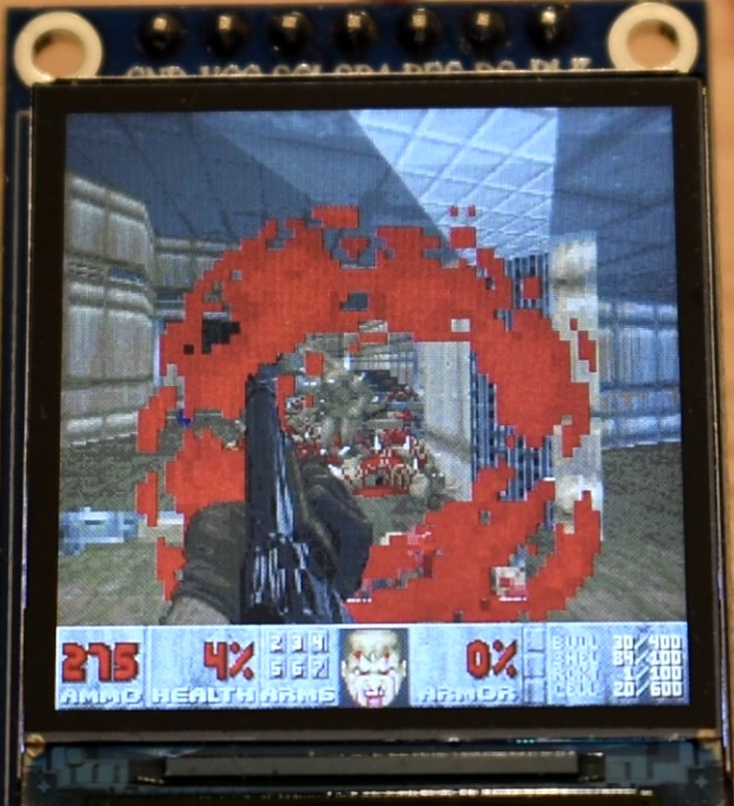
- The useless but very iconic screen melt effect, so far missing on the unofficial Doom port to the GBA by doomhack (on which this port is based), shall be restored. Since we are using a double buffer, with a simple trick it should come almost for free (a part some code reworking). This trick will have a drawback: the screen melt effect will be slower than the actual 3D rendering, as we explained in Appendix B.
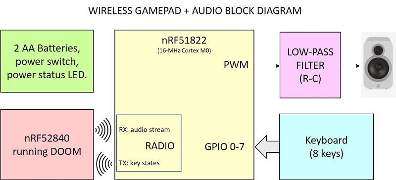
- Any “reasonable” hardware can be added for the keyboard/gamepad. As we will discuss later in this article, there are no enough pins to put an external keyboard, not even using a shift register. Since we are using an RF microcontroller, we can create a wireless gamepad. This means using… another RF microcontroller. We will be using the cheapest one we can reasonably find.
- Glue logic can be added, if we run out of pins.
- The nRF52840 found on the dongle must be the microcontroller that runs Doom. While another microcontroller can be added for the keyboard, it must not perform any Doom-related task, which would offload the main microcontroller.
- No RAM can be added.
- Since we have an USB dongle, the WAD file shall be uploaded via USB. There is no restriction on the upload method: CDC or MSC are all acceptable.
- WAD files can be modified to speed up data processing but no changes on the graphics details, maps, etc. shall be made. In other words, for instance, even if we pre-convert integers to fixed point values, everything (sprites, level, behavior) must look exactly as the original Doom (of course without taking into account the different screen resolution!). That means: changing data format or any pre-calculation is acceptable, reduction-simplification of maps or any graphic detail is not (except status bar numbers and elements, which, like in doomhack’s port, were adapted for a 240-pixel wide display).
- Audio can be implemented in any way, using DAC, or PWM, or the audio stream can be even sent to the gamepad (like a Wii remote). PCM sound effects shall have the same quality as the original Doom, i.e. 8 bit, 11025 samples per seconds.
The WAD file Storage
To store the WAD file, we are going to use a 16 MB QSPI flash. 8MB are fine for the shareware DOOM WAD, but if you want to play the full DOOM, then 8 MB are simply not enough. 4MB are not enough even for the shareware version, as the DOOM.WAD will increase in size after conversion with our tool (this is a required step!), exceeding 4MB.
In our case, we used a Winbond W25Q128JV-series. There are many variants of that chip, but our code will take care to enable the QSPI mode and set the highest drive strength, so all these variants should work. Other devices from other manufacturers should work as well, as the QSPI interface is using standard flash commands. Anyway, these Winbond memories are amongst the cheapest ones we could find, so there is not really a good reason not to use them, unless you have already other 16MB QSPI flash ICs. This port does not support 32 MB memories (very little effort is required, but we expect a slower speed because 32 bits, instead of only 24, will be needed for the address).
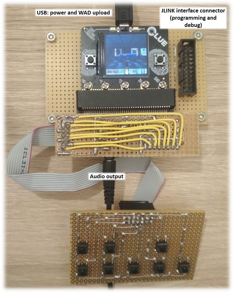
The Development Board
To develop everything we used an Adafruit CLUE board, which already integrates everything, except a large enough QSPI flash (the stock board only has a 2-MB flash). Yes, as a side effect of this project, we have ported Doom to the Adafruit CLUE board too!
If you want to replicate this project just on the Adafruit CLUE board, you need either to replace the soldered 2-MB flash or add an external one. As said before, we suggest to use a 16-MB flash, but 8 MB are enough for the shareware WAD (Note: we are talking about megabytes, not megabits!) . We show the all the details for the development board on Appendix C.
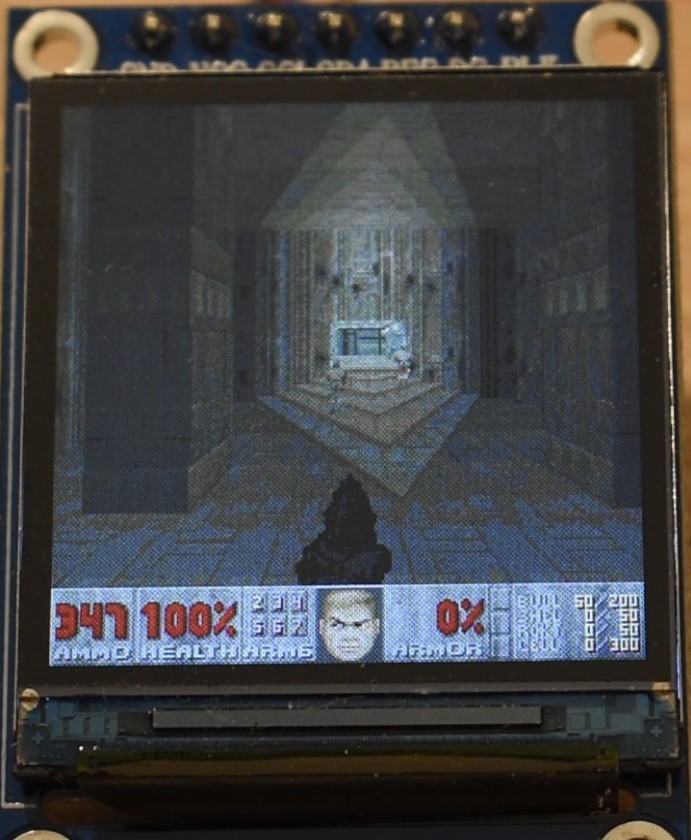
The Display
As we wrote, we are going to use a stamp-sized display, very similar to what you find on the Adafruit CLUE board. There are many reasons:
- That display is cheap, and widespread.
- The quality of the image is extremely high, especially if we compare it to the 160×128 pixel display.
- No need to overclock it. The ST7789 display controller can go faster than 32 MHz.
- 240 is a number that fits well in a byte. 320 does not. This is useful because some data structures such as “drawsegs” and “vissprites”, which make uses of horizontal coordinates.
- Still 240×240 pixels is a decently-sized resolution. As discussed in the Appendix A, in terms of 3D rendered pixel (i.e. not counting the 32-pixel tall status bar), we have about 92% of the original DOOM resolution and 325% of the unofficial GBA port by doomhack. Remember these value, as they will be discussed later!
- Last but not least, since the Adafruit CLUE was our development board, keeping the same display was very convenient for obvious reasons.
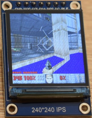
This display is typically soldered to cheap breakout boards. Some of them provide the full SPI interface (i.e. chip select, clock, slave input), along with the data/command and reset lines. Some other, provide a reduced SPI interface, because they internally force the chip select line to ground. This latter configuration is quite odd, as while the reset can be issued using an SPI command (i.e. reset pin is redundant), the unavailability of chip select will not allow using the display in a multi-slave SPI bus. Luckily, in our project we are not using this feature. Display boards with this latter kind of solution were cheaper, and we used these ones.
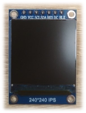
Note: the display shown above, uses SCL for “serial clock” and “SDA” for serial data, however they should be called SCK and MOSI, respectively, to prevent confusion with I2C signal names. In this article, we will use SCK and MOSI.
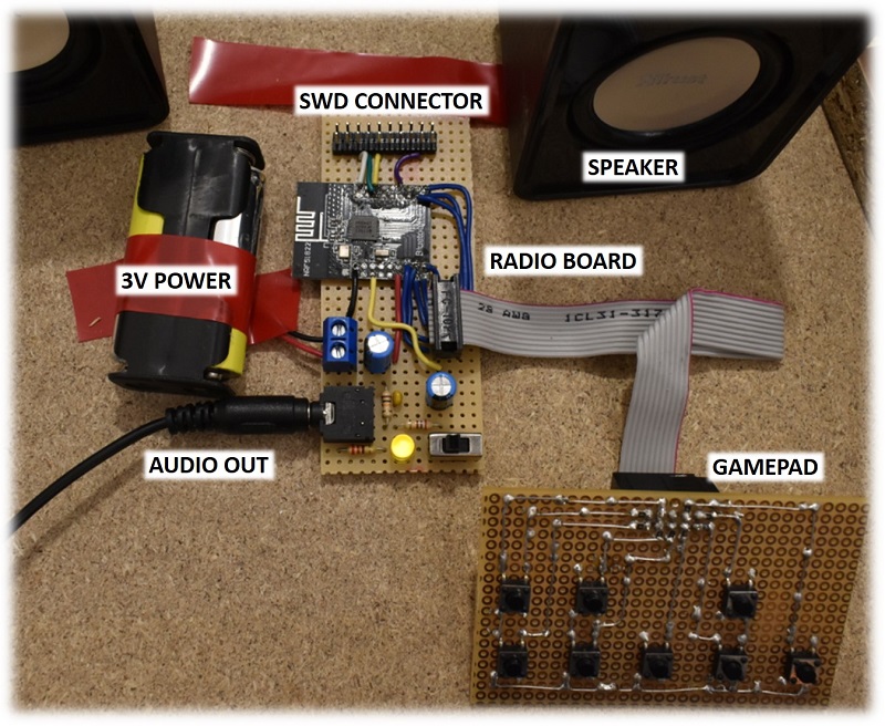
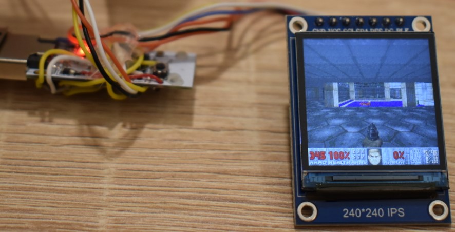
The Target Device
This is the final device on which we want to run Doom:
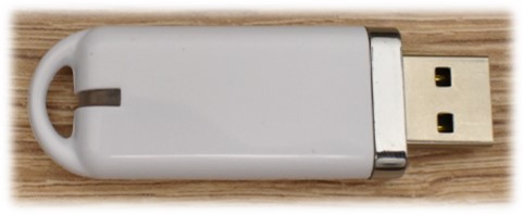
Form the pictures below, you can clearly see it is based on the nRF52840 RF MCU.
Noticeably, the nRF52840 is used in many other devices, such as 50$-100$ computer mice. In this project we wanted to keep everything cheap, and use the simplest device we could find.
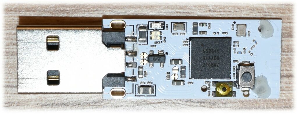
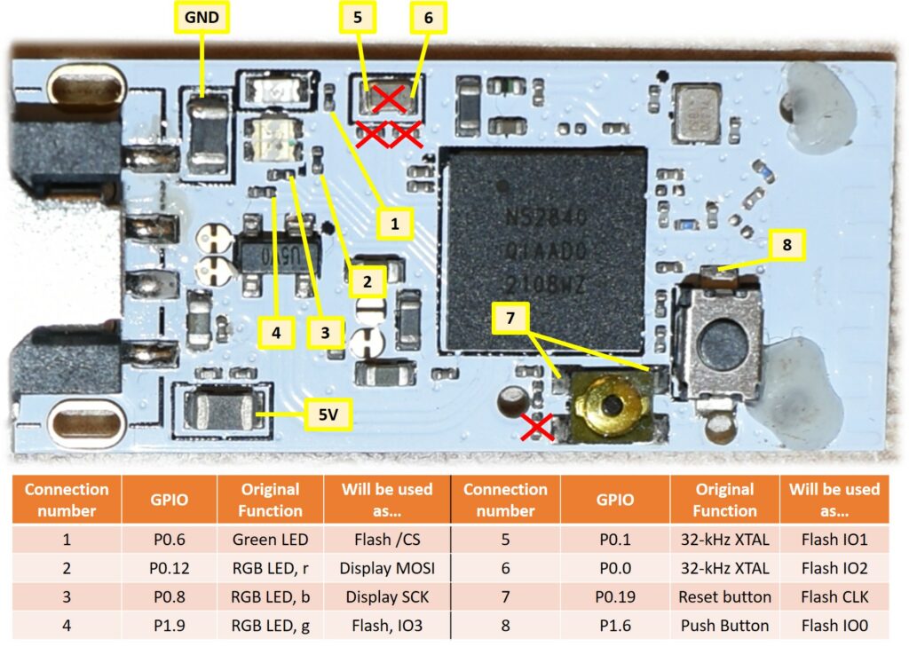
Unfortunately, the nRF52840 package variant used in the target device does not allows us to access unconnected GPIO very easily, because its contacts are on the bottom side, and they do not extend toward the package edge like a normal QFN.
For this reason, we can only use those pins that were routed out by the designer.
We identified 8 possible GPIOs:
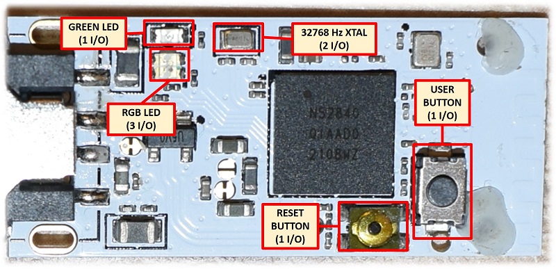
- Four of them are used by 2 LEDs (one of them being RGB).
- 2 GPIOs are used by the 32768 Hz crystal, which we are not going to use.
- There are two push buttons, one of them could have been used for the reset function. Never mind.
The exact port at which these signals are connected where discovered by attaching an SWD debugger with Segger Embedded Studio and writing to the port registers, to see when those signals changed from 0 to 1 and vice versa.
Luckily, the USB lines are routed as well (of course, being the device a USB stick!). We will use the USB to upload the converted WAD image, using a custom CDC interface implementation.
Let’s count how many pins do we need (let’s consider that the gamepad will be wireless. After all, we have an RF micro here):
- QSPI: 6 pins (CLK, /CS and 4 I/O)
- Display: 4 pins (CLK, MOSI, D-C and one between /CS or Reset).
- Audio: 1 pin.
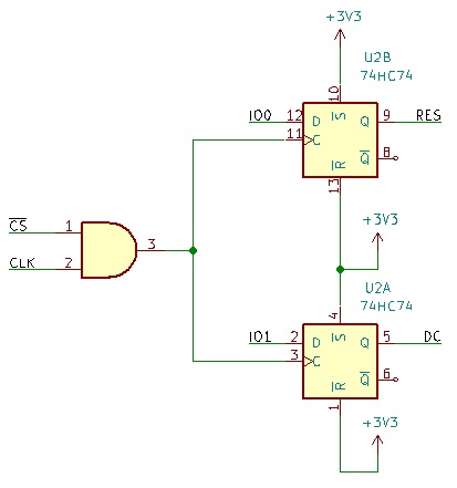
Eleven pins ? We are short of 3 pins! There are a number of optimization possible. The easiest one comes out by looking at the QSPI interface. When the flash chip select is low, the QSPI chip is selected, and all the pins are used by the QSPI flash itself. However, when the flash chip select is high, the clock does not make any transistion, and in particular it remains low.
We can therefore use the flash chip select to “gate” the clock, and feed it to the clock input of two edge triggered registers: a single good old 74xx74 IC! The data input of these registers can be any one of the 4 QSPI I-O lines, and the outputs would be connected the display chip select (or reset) and D-C lines. When the flash is selected, the clock input of these register will stay low, therefore no data will be latched. When the flash is not selected, we can manually pulse the clock, to latch data and set the desired display chip select (or reset) and D-C levels.
Now there is a good news: we need to change the levels of the display /CS (or reset) and D-C lines only during the initial configuration. After the display is configured, D-C will stay high, and /CS will stay low (reset high), because to continuously update the frame we just need to send the RGB pixel values one after the other. When the end of frame has been reached, the display controller ST7789 will automatically point to the first pixel, so we can continue send the data for the next frame, without any intervention on our side.
That said, this is our strategy: we first configure the display keeping high the flash /CS and pulsing CLK to latch the correct display /CS (or reset) and D-C levels, and later we will initialize the QSPI interface. After the QSPI has been configured, the flash clock line will never make a transition when the chip select is high, so the display /CS (or reset) and D-C will stay at the preset levels.
This trick will slow down the initialization, (by some ms using the /CS and by 150 ms using the reset signal) but no one will notice. By the way, we used a 1-ms resolution in the delay function, and actually, using a display with the /CS signal we could have gone much faster than this. Still no one would be able to appreciate the difference. It remains to understand how can we “gate” (inhibit) the clock, when the /CS is low. For this, we are using two diodes and a resistor, to implement an “AND” gate. When any of the signals is low, the output is low. In particular, if the /CS is low, the register will see a low clock value. The clock, seen by the register can become high only when the /CS is high, and the CLK becomes high as well. This will occur only during initialization, when we use the CLK as GPIO and manually change its state, because when the QSPI module is running, the CLK will never make a transition when the flash /CS is high. Problem solved.
NOTE: as you might see from the display picture above, we bought some modules without chip select, as these were cheaper. The initialization is quite longer (150 ms, barely noticeable), and the SPI must be configured in mode 3. This is already handled by our code. Luckily, the display is not sharing the bus with other peripherals, so it can be still used without problem. If you have a display without reset line, you need to set to 0 the definition of DISPLAY_USES_RESET_INSTEAD_OF_NCS in main.h. If you have display with both chip select and reset signals, then you can simply connect to ground the chip select, and leave the source as it is now.
Ok, we freed 2 pins, but we needed 3 more, not just 2! We are solving this issue in the next section!
Gamepad and Audio
For the Adafruit CLUE there are not many issues, as its Micro:bit edge connector has many I/O, and several options exist for the gamepad. Audio is simple as well, we just used one pin connected to the PWM unit and a low pass filter. For more information about this, see Appendix C.
What about our target device, i.e. the BLE dongle? As we said, the gamepad shall be wireless. In fact, we have an RF microcontroller here! Using the built-in radio is not that hard, especially if you are not using any protocol like Bluetooth etc., so we can implement a poor’s man wireless gamepad.
In the code on github you can chose between several gamepad implementations: parallel, I2C port expander, and RF-based. Of course, the non-wireless options are available only on those devices with many routed I/O pins. The wireless gamepad option is available for the CLUE board too.
And what about audio on the target device? Let’s stream it to the wireless controller, like the Wii remote! This saves one more pin, so the 8 GPIO pins on the BLE dongle are definitely enough.
Of course, for the wireless gamepad we need another radio board. We can use the cheapest board we could find in the market, based on the nRF51822, a 16 MHz Cortex M0.
The cheapest one we found is shown below.
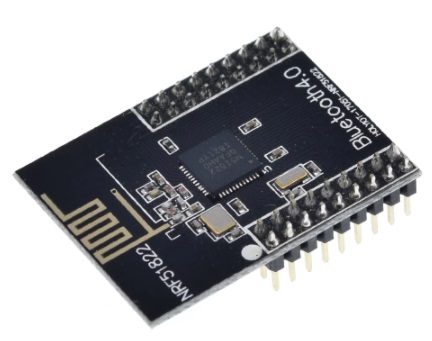
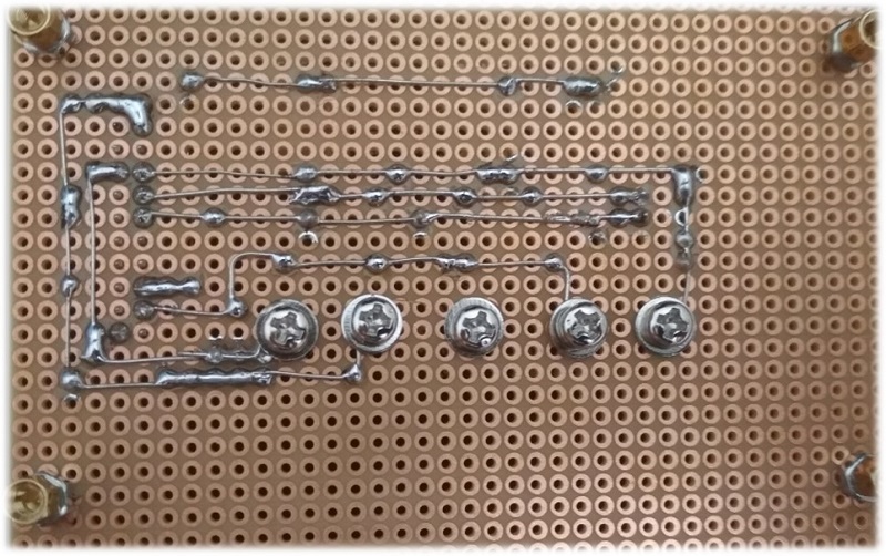
We have connected it to a simple keyboard (it looks familiar, uh? 🙂 ), two AA batteries, a power-on LED, the debug connector and the audio section. Noticeably, we removed the 2-mm headers and we soldered pins directly to it. In fact 2-mm female headers are much more expensive than the RF module itself!
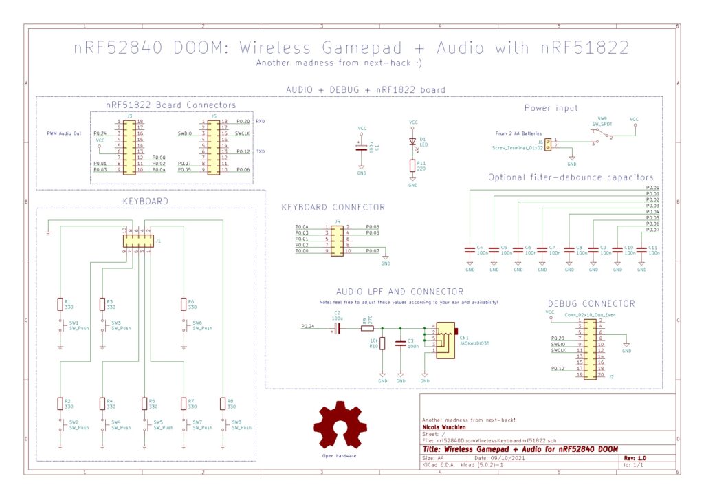
This is the schematics of the prototype above. We have indicated the GPIO pins we used, since you might have another module with the same MCU but different layout.
Noticeably, a 16 MHz Cortex M0 is definitely more than enough to handle key presses readout and audio playback, and it will have some spare CPU time too. You might want to add some extra functionalities, e.g. some RGB LED that flash in red when you get damage or change color when firing or getting a bonus.
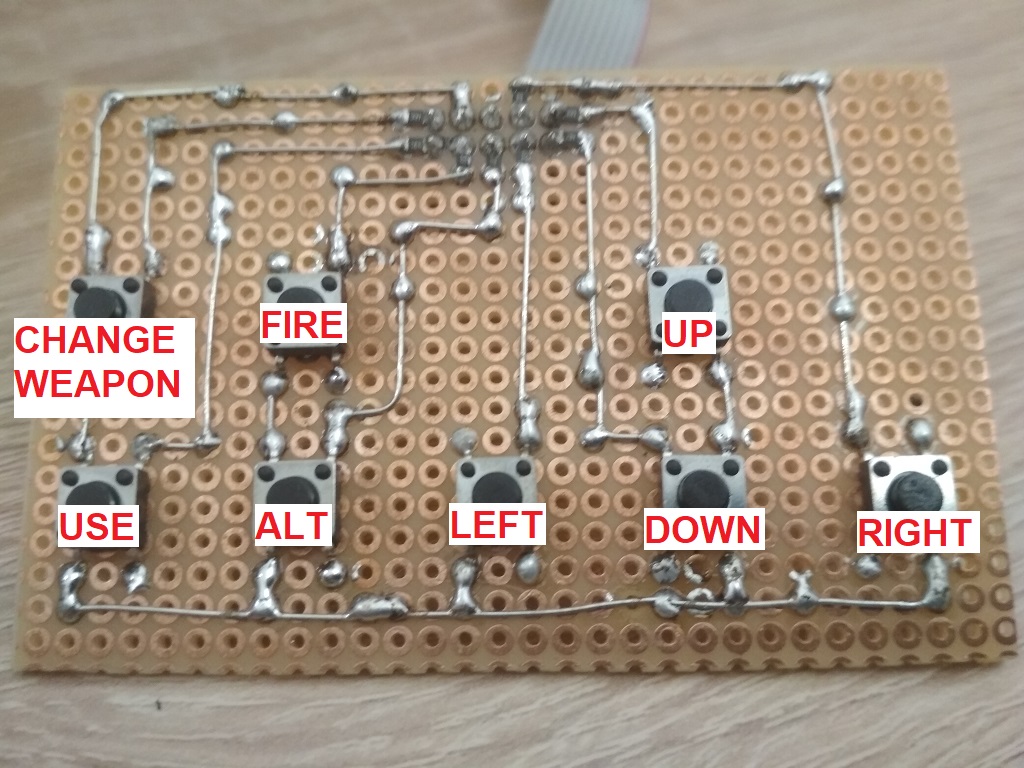
This is the keyboard layout we used. We used the same board also when developing everything using the I2C solution on the Adafruit CLUE.
Some details about how the wireless gamepad and audio are implemented can be found in Appendix D. The code is of course on the github repository.
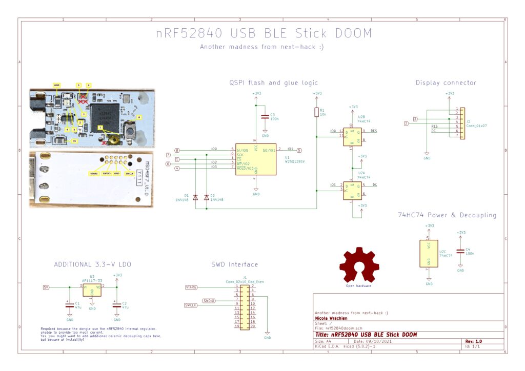
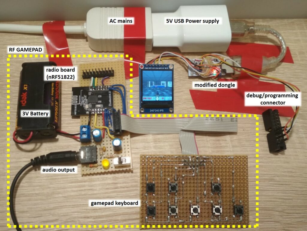
Target Device Hardware Modifications
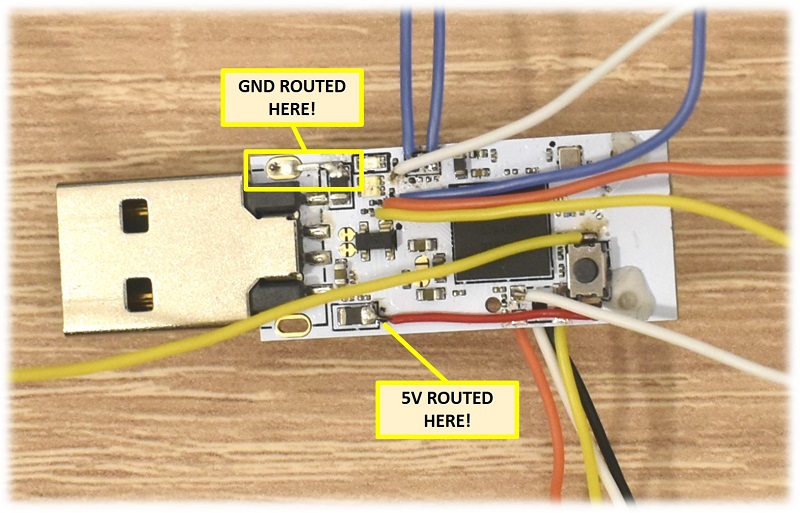
The USB stick need to be opened, and some wires need to be soldered to the tiny pads, as shown in the picture below. You do not need to remove the LEDs or the pushbuttons (we removed one just for reverse engineering and counting the number of available pins). These can stay in place, and the LEDs are also funny to watch, as they will change color, based on data. However, you have to remove the crystal and loading capacitors, as well as the other capacitor close to the reset button, indicated in the picture below with the red “X” marks.
We used silicone stranded wires, because these are very flexible, so less stress is applied to the solder joint when they are handled/bent.
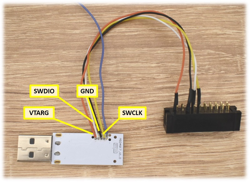
As a first step, we suggest you to have a connection to the debug interface to test that everything is fine. For that reason you must solder some wires to the SWDIO, SWCLK, Vtarget and GND pads on the bottom side as we did below. Instead of soldering, you might also use an expensive 10-needle SWD probe from SEGGER. You can guess what solution we chose.
After soldering all the wires, we suggest to use hot glue, to reduce even more the chance of breaking one solder joint, during the following steps.
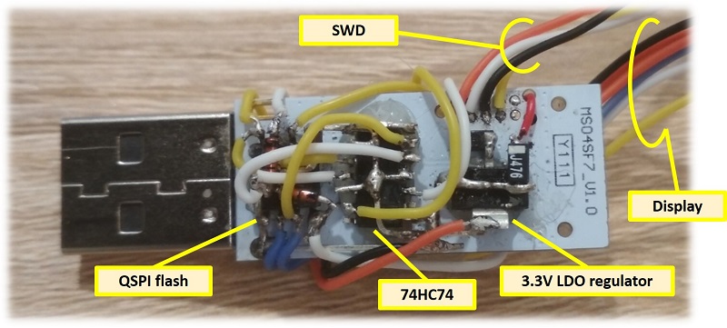
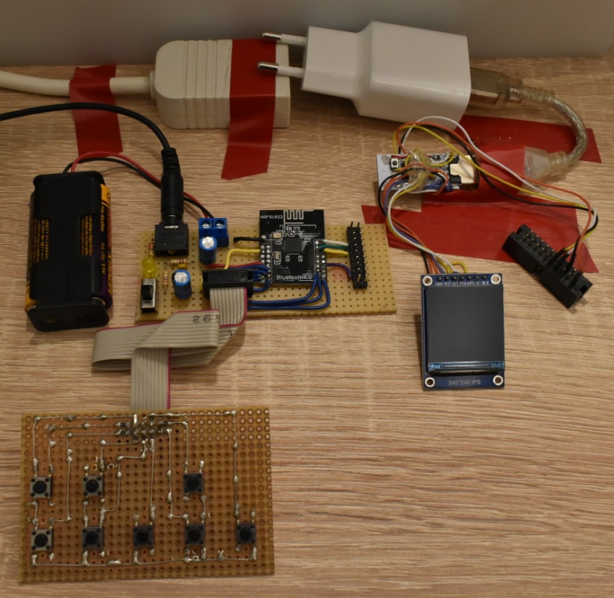
We could have done a PCB, and maybe in the future a simple one will be done as well. However, for the first prototype, we decide to put all the components on the backside of the board. For this purpose, we used hot-glue to fixed the three ICs, mounted in a dead-bug style. Beside the QSPI memory and the 74HC74 we put also a 3.3V voltage regulator, because the nRF52840 on-chip voltage regulator cannot provide enough current for the whole system.
The result is quite a mess, but it is working. That’s what counts.
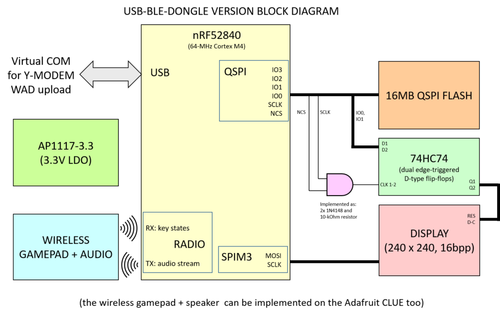
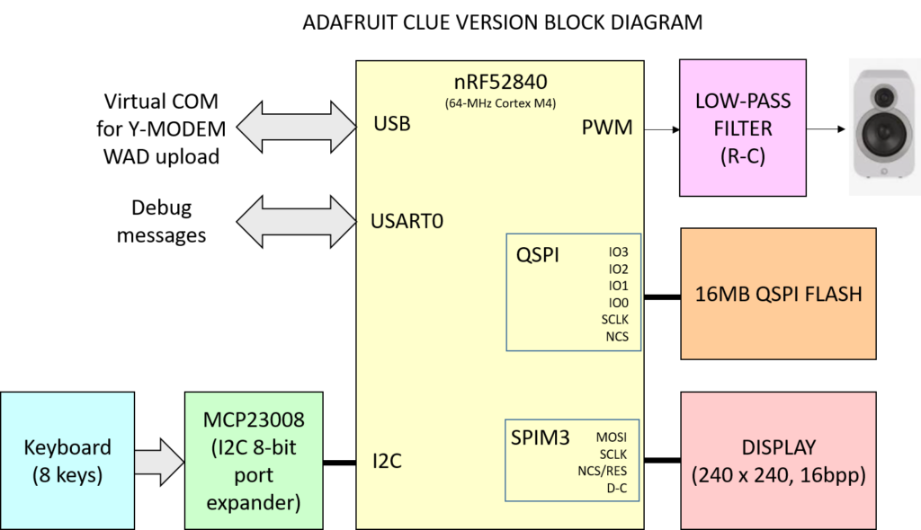
The block diagram and schematics are shown below.
The audio+gamepad schematics are shown in the gamepad section.
For the wireless gamepad schematics, refer to the previous section gamepad and audio.
Here’s the complete system!
The Software
This project is actually split in 3 different subprojects:
- The actual port, i.e. the firmware for the nRF52840.
- The wireless gamepad.
- The WAD converter.
In this section we mostly describe the nRF52840 firmware, with particular emphasis on speed and memory optimization. Details about the wireless gamepad firmware and audio can be found in Appendix D, while the WAD converter is briefly explained in this section.
The actual port is based on our previous project on a CM33 micro, which, in turn, is based on the excellent doomhack’s Gameboy Advance (GBA) Doom port. Beside the obvious low-level hardware-related drivers, we made later some substantial modifications to significantly improve speed.
Speed optimization
This time, not only we have a slower MCU, but also a larger display resolution. To get a good frame rate, we need to perform some optimizations. Here we discuss some of them.
Double buffering and DMA based display update
As previously mentioned, we implemented double-buffering so that we can render the new frame (in the back buffer) while the DMA is sending to the display the previous one we have already calculated (in the front buffer). After both DMA and rendering are done, the roles of the two buffers are exchanged. Details about implementation are shown in Appendix B.
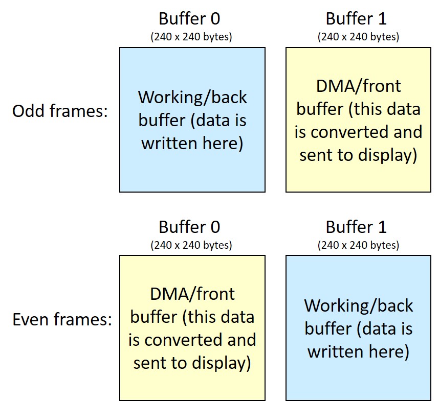
While double buffering uses a lot of memory (each buffer takes more than 56 kB), the performance gain are dramatic, as we show in Appendix B. For instance, if, with double buffer, we can render a scene at 30 fps, without it the frame rate would be just 18 fps.
Optimizing QSPI access time
QSPI usage optimization was another task to improve speed.
In fact, despite the QSPI interface allows to access the external flash as a memory mapped device, as we show in Appendix E, it is not very well suited for non-sequential accesses, which might occur during 3D rendering.
Therefore, when rendering the wall and sprites, instead of reading the column data directly from the QSPI, we first copy the column data to a RAM buffer, and then we feed this buffer to the column rendering function (sprites and walls are drawn column-wise). We found this is much faster than trying rendering data directly from the QSPI, despite the additional “copy-to-RAM” step.
We also modified the patch format so that the column offset array (“columnofs”) also contains the size of the column in bytes. This useful for masked patches (i.e. sprites or textures with transparent pixels), because it allows to load an entire column via DMA, without having to “parse” it using the CPU.
Using the DMA has another benefit: double buffering (again). While the QSPI is loading to RAM via DMA the column data, the CPU is free, therefore we can implement a double buffer here too. In particular, we modified the code so that all the sprites and all the wall textures are drawn using a double buffer for columns. Thank to this, when we are drawing one column, the DMA can fetch the data from the QSPI to RAM, at the same time, noticeably increasing speed.
As a final optimization, when drawing masked patches, we check how many columns we are going to draw. If this number is large enough, we load to RAM the whole patch column offset table, instead of getting it by column basis. This saves a lot of CPU cycles, because every column offset readout would be seen by the QSPI as a random-read operation, which produces a 4.5-us delay.
Caching to internal flash
As we will explain later, we save to the internal flash some data, which won’t change unless you upload a new WAD file. Since these data are constant, it would be wasteful to use precious RAM, therefore the internal flash is a good place for them.
However, if we stored only such data, we would leave our internal flash more than 2/3 empty. Internal flash can be random-read much faster (requiring only up to 2 wait states, i.e. 4 CPU cycles per data access), with respect to the QSPI, which suffers a lot in random-reads. Unfortunately, many drawing operation require non-sequential reads (one for all: floor/ceiling drawing), and having the data in the QSPI would kill performance. For this reason, we copy all the level floor and ceiling textures to flash.
This would still leave some hundreds kB free, which we use to store as many wall textures as possible. Those wall textures, which cannot fit the flash, can be still copied reasonably fast, as we explained above, using our QSPI optimization technique.
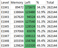
Flash usage will depend on the WAD and level. In the picture below, we report the flash memory usage on the level E1M2, from the Ultimate Doom WAD file (converted with our tool).
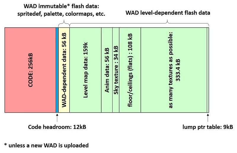
In the figure above, the code occupies a quarter of MB. A small headroom is inserted so that small modifications would still fit. This also ensures that the cached data (immutable + level dependent) are page aligned (4kB). After the headroom we place all the data that do not depend on the level being played, for instance the color maps, palette and spritedefs (data structures that determine the number of frames of each sprite, the lump number of each rotation frame, and if some frames are flipped). Next we find the actual level map data, the anim data and sky texture (which depend on the episode). After that, we find all the floor and ceilings used by the level. Then we cache as many textures as we can, while still reserving a region for the lump pointer table (whose size is known a-priori, when the WAD is parsed). The lump pointer table is saved at last. This is because we can know the pointer of each lump only after we know which textures we were able to cache into the internal flash. For all the other lumps, that were not cached to internal flash, we use the pointer to the external flash.
Noticeably, caching to flash increases a lot the level-loading time, which can be as high as 20-30 seconds. This is a very long time, but the benefits in terms of playability are extreme.
Note that writing many times to the internal flash will have some impact on its reliability, but as shown in Appendix F, the effect is very limited for practical usage.
Composite texture optimization
Composite textures are among the heaviest things in the Doom code. Put simply, these are textures made of different graphics elements (called patches). This allows to re-use the same patch in the same or other textures, saving a good deal of space, at the expense of performance. For instance, in a composite texture, patches might overlap, and this generates some overhead, which noticeably reduces the performance if some strategy is not taken, as we will discuss below.
Below we show an example of composite texture, with overlapping patches. It is made of 10 patches. The rectangular back plate patch is repeated 4 times horizontally, and, on top of the first 3 patches, we find six screens. The edges of the patches have been highlighted.
Both doomhack’s GBA Doom port and the Nordic nRF5340 one implement some variations of composite texture caching or pre-calculation found in all the Doom ports. The GBA one implements a 4-way associative cache, with random eviction strategy in case of cache miss. Instead, the Nordic port will pre-generate all the composite textures, and will store them to the QSPI flash, at startup.
We decided instead to go for a different way, acting directly on the WAD: multi-patch textures are converted to a single-patch one, which contains all the graphics data (no detail is lost), using our WAD converter. Therefore, for each multi-patch texture, a new rectangular solid patch will be added to the WAD, and to its PNAMES lump (PNAMES, which stands for patch names, stores the list of all patch names in the WAD). All this will result to a big increase of the WAD size, because while with the same “few” patches you could create many big textures, now each texture needs its relatively big patch. For instance, using the commercial DOOM.WAD, the size increases by about 1.2 MB.
Flash caching will be also less efficient, because instead of caching many small patches, we will be actually caching big patches corresponding to pre-generated composite textures, therefore fewer textures will be actually cached. This means that fewer texture data might be already on flash, i.e. fewer textures can be read at high speed. However, this slow-down is offset by the speedup we get, because no multiple patch fetches and composite column generation are required anymore. Furthermore, since all the textures are now single-patch (whose size is exactly the size of the texture itself), the column loading is very fast, as the size and column offset are known a-priori, without requiring to load any data from the columnofs array.
This pre-generation slows down the one-time WAD upload (due to its larger size), however it will increase level loading speed as well.
Other optimizations
We made many more optimizations, some of which will be briefly cited here.
We modified the floor and ceiling drawing routine. On the GBA port, each pixel was calculated and directly written to the display buffer, using a store byte instruction[1]. A store instruction is expensive (it takes 2 CPU cycles), therefore instead storing the result directly on the display buffer, we put the first pixel in a CPU register. The successive 3 results are added to the same register, using an SHIFT+OR operation (This is done in a single cycle, because the ORR instruction allows to shift the source register by an arbitrary amount). Finally, the 4 pixels contained in this single register are stored to the display buffer. This last store operation can take at most 3 cycles (because of possible unaligned access, otherwise only 2). This allows saving up to 3 cycles every 4 pixels.
Another optimization came from leaving as much flash free as possible to use it as caching, as explained above. This is easily achieved, by setting the “optimize for size” to the whole project, while leaving only the files responsible of drawing-related functions as “optimized for speed”. This allows to keep the code size small enough, so that most of the internal flash can be used to cache textures, which can be accessed much faster than the QSPI.
Finally, let’s talk about the most recent optimizations: color map caching and optimized 8 to 16 bpp conversion, used to update the screen via DMA (see Appendix B).
For the first one, we reserved a 256-byte buffer for the colormap. The colormap is a table that, based on the lighting, will map the original texture color indexes to their darker version in the palette. Putting all the colormaps to RAM would require 8.5 kB, so we keep them in the internal flash. However, the internal flash requires more wait states than RAM, therefore, if we need to consecutively draw a large enough amount of pixels with the same color map, we copy the 256-entry color map to RAM (this operation occurs nearly at 128MB/s!), so the access speed will be faster. Next time we are drawing some other pixels, we check if we are using the same color map, and we will use that instead, without copying it.
To optimize the 8 to 16 bpp buffer conversion routine, we analyzed the assembly output, and we found it was very unoptimized, requiring more than 2200 CPU cycles per line buffer (as explained in Appendix B there are 225 256-pixel line buffers), i.e. 7-8 ms per frame. To optimize this, we considered the CM4 Load-Store instruction set timings, and we exploited pipelining to achieve the best performance. Now the conversion requires about 1000 CPU cycles per line buffer (i.e. less than 225000 CPU cycles per frame, i.e. about 3.5 ms). In othe words we saved at least 3.5 ms per frame: this corresponds to the difference between running at only 30.8 fps and a 34.5 fps.
Memory optimization
The bulk of memory optimization was made on the previous work, where we had less than half the memory we have now. However, only thanks to this optimization work, we were able to implement some of the most important speed optimization discussed above (in particular double buffering).
In fact, it is worth noting that the GBA has 384 kB of RAM, i.e. 50% more than what we have. In fact, in the GBA we find 256 kB of main RAM, 32 kB of IWRAM (a 32-bit fast RAM, internal to the MCU), and 96kB of video RAM. In the GBA port, the RAM usage is still quite high, if we compare to what we have available here.
We can easily show this using the memory consumption data reported by doomhack for various levels.
Note that these data do not take into account the memory block overhead (which might be as high as 14kB, just considering the objects present on the most complex levels), the memory used on IWRAM and the frame buffer. In some cases, the memory consumption (not counting overhead and frame buffer) would have been close to 200kB, as for instance in level E1M6. Adding the 56kB required for just a single frame buffer and the aforementioned overhead already exceeds the 256-kB limit.
Instead, with the optimizations made in the previous work, the zone memory occupation typically was under 75kB on E1M6 (the maximum available zone memory was 78600 bytes). The now available additional RAM allow not only to implement a double buffer for the 240×240 display, but also to increment the zone memory size and some static limits, as we will briefly discuss later.
Here is the (incomplete) list of optimizations we made previously, and kept in this work.
- Doom code used extensively 32 bit integers, where 16 or 8 bits were enough. Similarly, many 16-bit variables were used, when less bits were enough. Bitfields were used as well for those integer requiring fewer values.
- Enums were used very frequently, but these are usually implemented as 32-bit integer. Instead of using enum data types, we trimmed the data size to be enough to store the largest value.
- We reordered many structure members. Structure reordering saves space due to lack of padding bytes required to align 16 or 32 bit members.
- In the GBA port, several tables were copied to the IWRAM region, to increase speed. We kept them in flash.
- Pointers. This would deserve an article on its own, but the key point is: why do we need a 32-bit pointer, if our RAM is 256kB ?
Furthermore, almost all pointers point to 4-byte aligned structures. This means that a 16 bit pointer would be enough (we do not need to store the lower 2 bits, being all zeroes). Therefore, many pointers were replaced by 16-bit short pointers. Setting and getting data will of course require more CPU cycle (To convert a 32 byte pointer to a 16 bit and vice versa), but a 64 MHz MCU is much more powerful than a 16.8 MHz ARM7, so this should not be a big deal. This is probably the most important memory optimization. - We reverted PrBoom Z_Zone to an implementation much closer to the original one (removing useless stuff like Zone Id, and using 16 bit pointers, to save several kB when you allocate many buffers). Why? Because PrBoom’s Z_Malloc() uses the stock malloc/free functions, which on their own store memory block data (8 bytes, typically), further wasting memory.
- The object structure (mobj_t) in Doom is huge. On the GBA port was 140-byte large, and we reduced it to 92 bytes, already saving many kB on the more complex levels, like E1M6 (463 objects). However, some objects, like bonuses and decorations, are static, and do not need all the information required by enemies, bullets, etc. Therefore, we created also a static mobj type, which cuts to half the memory requirements (its size is 44 bytes). In some levels, there are more than 200 of such objects. These optimizations saved more than 30kB of RAM in E1M6.
- We used memory pools (used only for msecnode_t data in the GBA port) for objects (mobj_t and static_mobj_t). This reduces the dynamic allocation overhead to 1 byte/object for pools as small as 16 entries. To achieve this goal we had also to optimize memory pool allocation system as well. This reduced further the additional cost of each mobj/static mobj by 27 more bytes per object.
- When possible, 8 or 16-bit array indexes were used, instead of pointers.
- Some information, such as switches textures can change during gameplay, so they need to reside in RAM. However, the number of switches in the game is very limited, compared to actual number of sides on the level. Static walls can reside in internal or even external flash. Therefore, for the switches, we created arrays to store changeable texture information, while other constant information are read from flash.
- There are some data in the WAD file, which require some additional calculations before they are used. Such data cannot be easily calculated at compile time, such as memory pointers (for instance, this occurs with some sprite data structures). In the GBA port, such data are kept in RAM, even though they will remain constant as long as you don’t change the WAD file. Instead, in our case we can save the results in the internal Flash (our programming algorithm will check if programming is actually needed or if the same data is already present), saving a lot of kB.
- doomhack’s GBA Doom code used 16 kB on the IWRAM to implement a software cache, to speed-up composite texture rendering. To increase speed (hit ratio), doomhack implemented mip-mapping, which decreased the level of details on composite textures. As discussed before, in our case, composite texture are optimized by pre-converting them to single patch textures, using the WAD converter. Our solution not only saves these 16 kB RAM, but also increases a lot the drawing speed, while having no effect on the texture details or complexity.
As previously mentioned, despite we used a lot of memory just for the framebuffer, we still had the chance to:
- increase the zone memory from 78600 bytes to 113600 bytes. These extra 35000 bytes can provide a big deal of safety margin, even on the more complex maps such as those found on Doom 2. Increasing the zone memory was also necessary because, as mentioned before, the “visplane” data structure depends on the screen width, and visplanes are allocated dynamically during gameplay. Taking into account this, we expect a somewhat bigger Zone memory usage (in the order of 10kB), which still will be lower than the amount of which it was increased. Noticeably, the audio buffer is now statically allocated, therefore the zone memory requirement decreased of 2 kB (in other words, with respect to the previous port, it is like if we increased the zone memory of 37000 bytes, and not only 35kB).
- Restore MAXDRAWSEG to 192 as in the doomhack port. This was required to flawlessly play Episode 4 on “The Ultimate Doom”.
- Increase the number of openings, see Appendix G.
- Restore the number of visprites (on-screen visible sprites) to 128, as in vanilla Doom.
Programming
In the github repository, you will find the Segger projects for the Doom port and gamepad, as well as the Code:Blocks project for the WAD converter. To use them should download Segger Embedded Studio (we used version 5.5), and that’s it. Note that each Segger Project file has several options, which might be file-dependent. If you want to use another IDE, take this into consideration, to get the best speed! You need an SWD programmer in order to upload the file generated when you build the project. A Jlink EDU[2] programmer is suggested, so that you can upload and debug the code directly from the IDE. Otherwise, if you want to upload manually the generated binary file, any SWD programmer is good as well. Of course you must program both the dongle and the wireless gamepad.
Note: reprogramming the dongle means to have a full chip erase. The memory of the BLE dongle is read-protected, so you can’t make a backup of the firmware inside it: you will be asked for a full chip erase.
Uploading the WAD: WAD converter and USB CDC
As said before, we implemented the USB CDC functionality to upload the modified WAD to the QSPI flash. The Ultimate Doom and Doom 2 WADs require about 5 minutes.
Noticeably, we did not use Nordic’s USB stack: we implemented a rudimentary one by ourselves. As a matter of fact, of Nordic’s library we just used the startup code, the register definition and the errata code, i.e. workarounds by Nordic to fix some issues they found in the chip. Bare metal programming was used.
To convert the WAD we created a plain C command-line application (no third party libraries, only the standard C ones), which in turn is based on doomhack’s GBAWadUtils. This application is available on the same repository of this project.
This application does the following:
- It adds some graphics optimized for 240-wide screens. These graphics come from the GBA Doom port and were made by doomhack and Kippykip.
- It changes some of the level constant data structures, so that they can be kept in flash, saving a lot of RAM.
- It changes the patches so that they include the column length information in bytes (rounded to the upper 4-byte boundary). As mentioned above, this allows to speed-up QSPI data fetch.
- It takes multi-patch textures, draws them to a single temporary buffer to convert them to single patch textures. This increases a lot the wad size (about 1.2 MB increase on the commercial WAD), but it dramatically speeds up composite texture drawing (because they won’t be composite anymore, and a single patch has to be read for the texture, without intermediate composite texture generation).
To use the application you need to find a WAD file (tested for now: shareware Doom, commercial Doom, The Ultimate Doom and Doom 2). Then you need to open a command line interface, and write:
mcudoomwadutil.exe UnmodifiedWadFile.wad ConvertedWadFile.wadFor instance, if you have put mcuwadutil.exe in C:\mcuwadutil\, and the wad to be converted is in C:\MyWads\doom.WAD, then you must write:
cd C:\mcuwadutil\
mcudoomwadutil.exe C:\MyWads\doom.WAD C:\MyWads\convertedDoom.WADNote! gbadoom.wad must be in the same directory of mcuwadutil.exe, because this contains some status bar digits graphics data, adapted to 240-pixel wide displays.
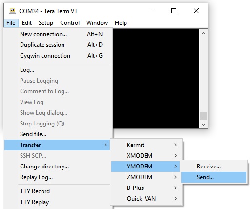
After you have converted the WAD file, you must connect your (already programmed) “Doom device” to the USB port of your PC, while keeping pressed for 2 seconds the buttons “alt”, “change weapon” and “use”. The “Doom device” will open a virtual COM port.
Then use TeraTerm, connect to the virtual COM port, and send the file using YMODEM protocol.
Note! Windows 10 natively supports virtual COM port devices without any drivers. Unfortunately, Windows 8 and earlier do not. You will need to find/create a driver for it!
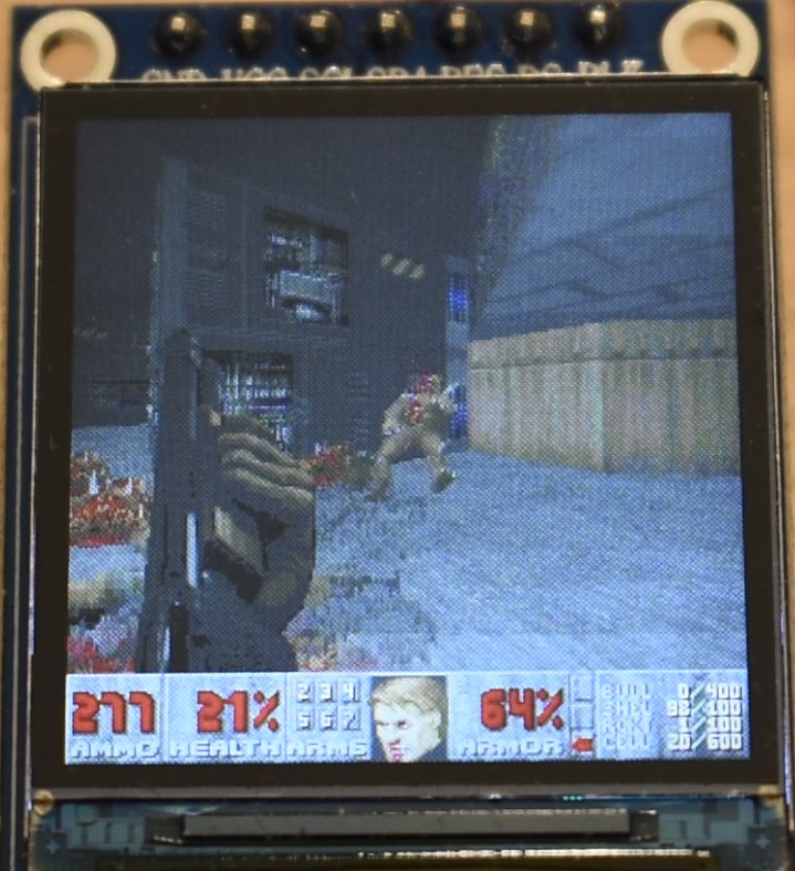
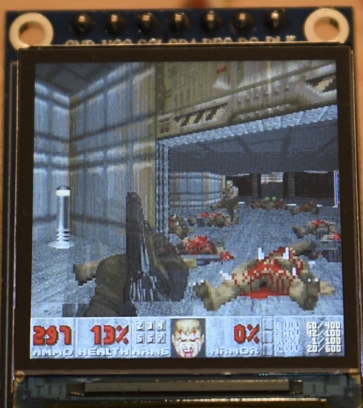
Image gallery and Video
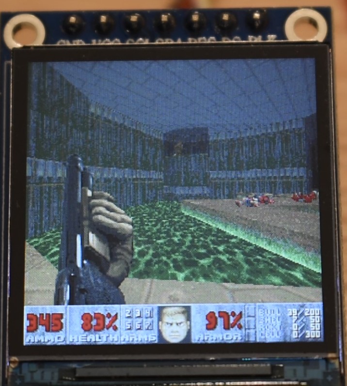
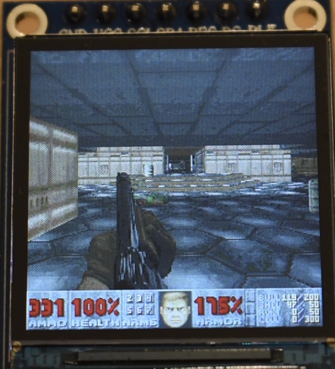
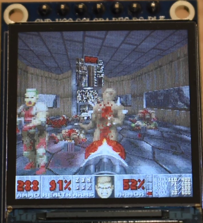
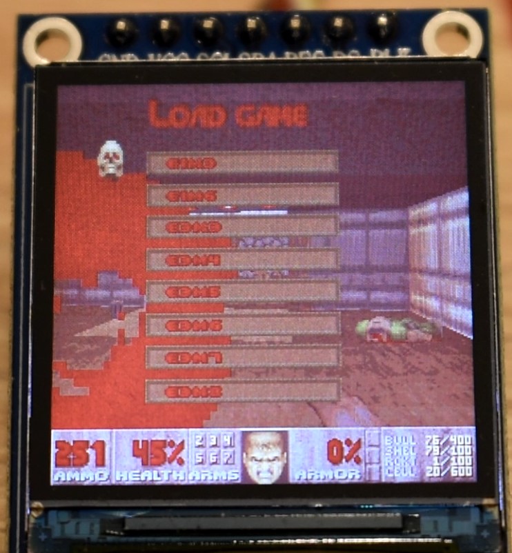
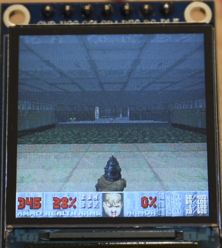
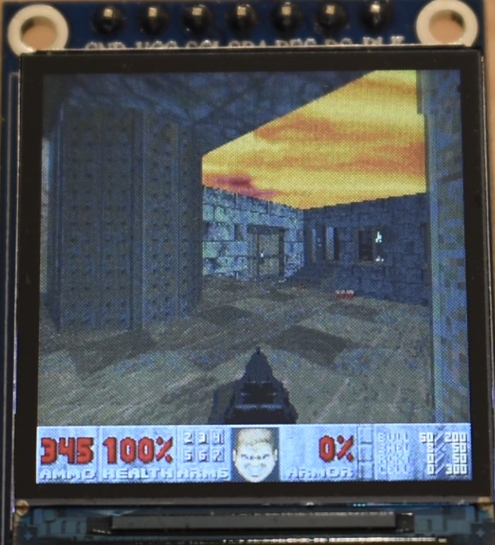
In the following you will find some images and the video. Note that:
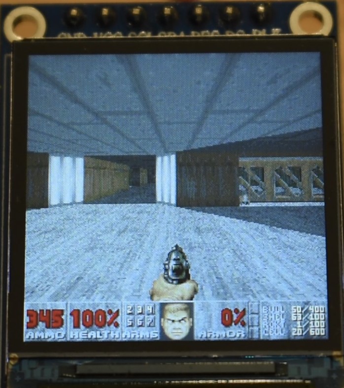
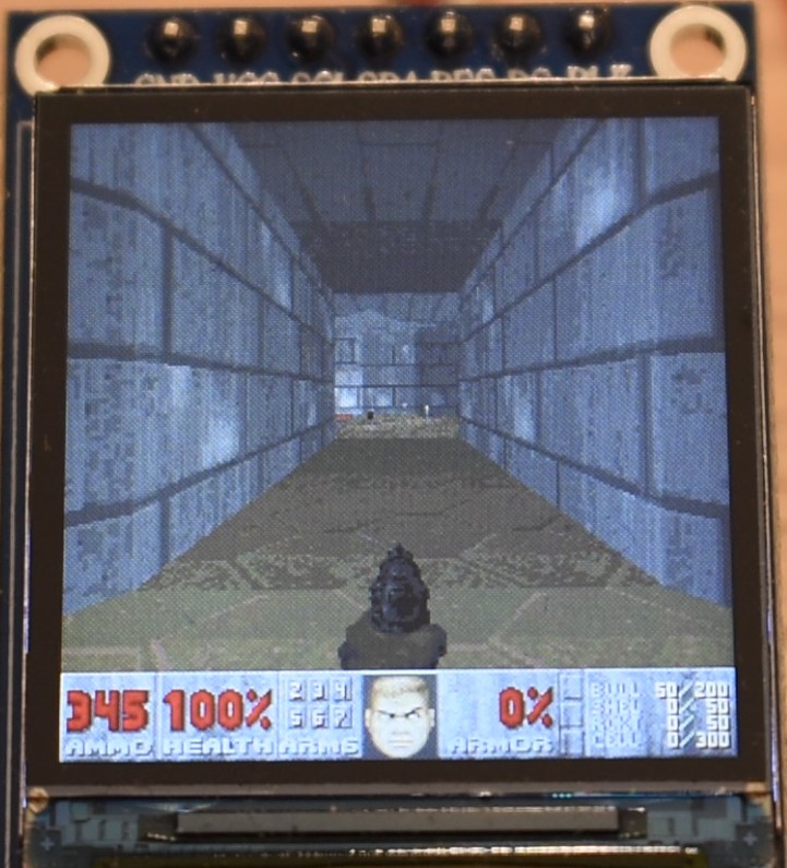
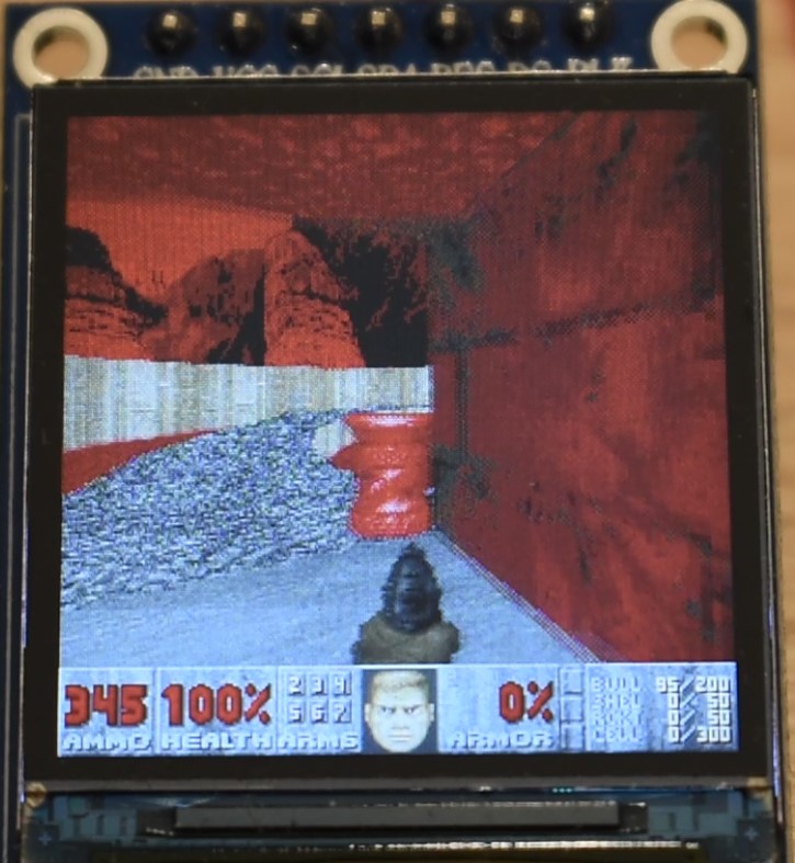
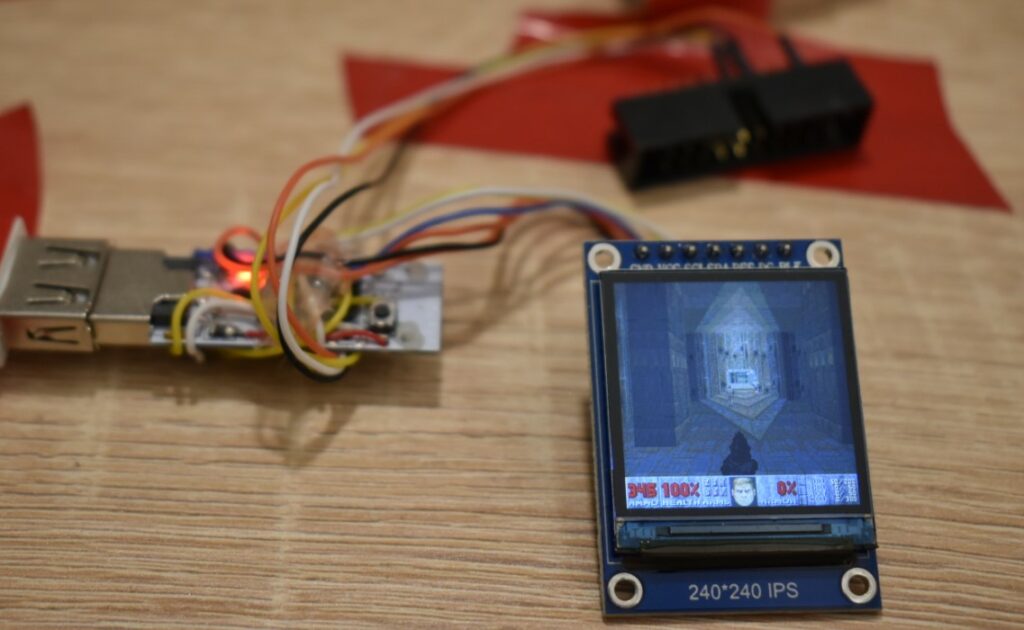
- In all the images and video, we are replacing the AMMO count with the current frame rate, multiplied by 10. I.e. 345 does not mean 345 bullets, but it means that the game was running at 34.5 fps.
- As explained in Appendix H, we are using a modified hardware gamma settings of the ST7789 display controller. This is because the factory defaults look wierd. However, we are using the in-game software gamma set to maximum (brighter images), for a number of reasons:
- Photos and videos are rendered somehow more easily.
- It is easier to appreciate all the details.
- It is easier to play, especially taking into account that, due to the video-shooting setup, we had to play the game at more than half a meter from the stamp-sized display. The brighter image allowed for an easier gameplay.
Performance
What about performance? Honestly, we were a bit pessimistic about performance, as 240×240 pixels are more than 3 times the resolution, in terms of 3D pixels, we had in the previous successful attempt, which even had a microcontroller 1.5 times faster.
However, with our extreme surprise and pleasure we found that, even without optimization, we got very playable frame rates, generally above 20 fps in all the levels, and often surpassing the 30 fps mark. After the optimizations and tuning we discussed above, the frame rate has significantly increased, at the point very often it is capped to its maximum value, i.e. 34.5 fps. Note that 34.5 fps is the hardware limit due to the SPI speed, as discussed in Appendix B. We show the results of our optimization and the final frame rates here.
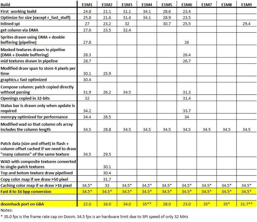
At this regards, a fair benchmark is difficult to get, unless the same tick-by-tick in-game events are reproduced on different runs. Since no demo is supported, what we wrote in the table is the fps we get at the beginning of each level at the lowest difficulty level. During our optimization work, these values were taken also as figure of comparison to assess whether a modification lead to better performance.
For instance, the initial frame rate on E1M1 was only 24.8 fps, and now is 34.5 fps: at least +39%. Similarly, E1M2, which is the slowest level of the original Doom game, started at 21.5 fps, but after optimization we got 34.5 fps: + 60% at least. Levels of Episode 4 are even slower, but these are not part of the original Doom release.
In more complex areas, the frame rates were as low as 18 fps before optimization, but now in the Vanilla Doom we can hardly find areas/scenes where the frame rate gets below 27 fps! In The Ultimate Doom episode 4, the frame rate is much slower, and it gets down to 20-22 fps in E4M2, i.e. the slowest map.
Performance Comparison with Other Ports
Comparing with other ports is always difficult, because, due to very different specs and features, we are not making an apple-by-apple comparison. Still, some ballparks figures can be found out. We will briefly discuss below the comparison with several other devices.
Unofficial GBA Port by doomhack
As already said, this port is based on the impressive Doom port to the GBA made by doomhack, therefore one might expect a similar level of optimization. Yes, we had to sacrifice some performance to save noticeably on memory (one for all: using short pointers) and to restore the Z-depth lighting, but we also made many optimizations that we believe largely overcompensate the aforementioned performance loss.
That said, Doom runs much faster on our device. At first sight, this is understandable: we have a MCU, which is about 5.3 times faster than the GBA ARM7TDMI clocked at 16.78 MHz. However, our port has 3.25 times the number of 3D pixels that are rendered on doomhack’s port, so this 5.3 speed factor should be reduced to 1.63 (5.3/3.25).
The question is: does our device run at a frame rate, which is 1.63 times the one reached by GBA? This is quite difficult to assess, for the following reasons:
- it is not clear how frame rate data are reported in this document (fps at first location? Some playthrough? And in which locations? ).
- When frame rate cap (either software or hardware) is reached, we cannot assess whether the device could have run faster, or if that frame rate was barely reached.
For instance, our device showed an almost constant frame rate of 34.5 on E1M1, whereas the frame rate reported by doomhack is 22 fps. For a fair comparison we should multiply 22 fps by 1.63, yieding 35.9 fps. Unfortunately, we cannto assess if, by removing any software and by having a faster SPI, we could have reached that frame rate.
A better example is level E1M2, where our port runs at 34.5 fps (first location), whereas doomhack port is at 16.0 fps. In the same level, the minimum frame rate we achieved is around 30 fps, i.e. faster than 1.63 times 16 fps. Still we can only provide a lower bound.
An even better comparison is on E4M2 (the slowest map). Our device runs at about 22.1 fps, while the GBA reaches 8 fps. The ratio between these frame rates is about 2.8, i.e. we can safely state that our port has a better optimization level.
However, we believe that this mght not be a fair comparison: doomhack’s port features music, an important feature we did not implement yet. Furthermore, we had tricks to increase speed (loading data using DMA, while drawing the previosly loaded column at the same time) and some code has been tweaked at the assembly level.
Still beside Z-depth lighting, our port removed mip-mapping (all textures are rendered at high detail) and restored the scree-melt effect. Useless, but very iconic.
We think that there is still some room for improvement on both sides
Nordic’s nRF52840 port
What about the port made by Nordic on 2019? Well, as written at the beginning of this article, our port has 92% of the 3D rendered pixels, with respect the original Doom resolution which is also the same resolution used by Nordic on their first 2019 attempt on the nRF52840. That said, our port is not running only 1/0.92 times (i.e. +9%) faster, but at least 10 times faster (i.e. +900%), therefore the marginally reduced resolution is not accountable for this huge speed boost. Incidentally, in their ports, Nordic used a FT810 video controller, which already takes care of receiving 8-bit indexed images, and converting them, using a 256-entry palette to 16 or 18 bits per pixel. This allowed them to leave the CPU free for additional time for the 3D rendering, and does not set hard-limit on maximum frame rate to 34.5 fps.
Nordic’s nRF5340 Port
What about the comparison with the port done by Nordic on the nRF5340?
Since the nRF5340 is at least 2 times faster than the nRF52840, one would expect that, when their port is running at 34 fps[3], our should run at 17 (or better, 18.9 fps, considering we only have 90% of their pixels).
Instead, by comparing their video, our port runs at the same speed or even faster [5].
Yes, on the nRF5340 the frame rate reaches some times 35 fps, while in our device we can “only” run at 34.5 fps, due to the maximum SPI clock frequency. Furthermore, our resolution is only 90% of the one used in the nRF5340 port , therefore, for a fair comparison, our 34.5 fps should be normalized by multiplying it by 0.9, yielding 31 fps. However, as stressed before, the nRF5340 is at least 2 times as fast as the nRF52840. Moreover, while for instance we get a nearly-constant 34.5-fps frame rate in E1M1, we can see from their video that the frame rate sometimes falls below 31 fps in the same level. For instance, as can be seen from the image below, the frame rate was about 24 fps, i.e. much smaller than the aforementioned 31 fps normalized figure.
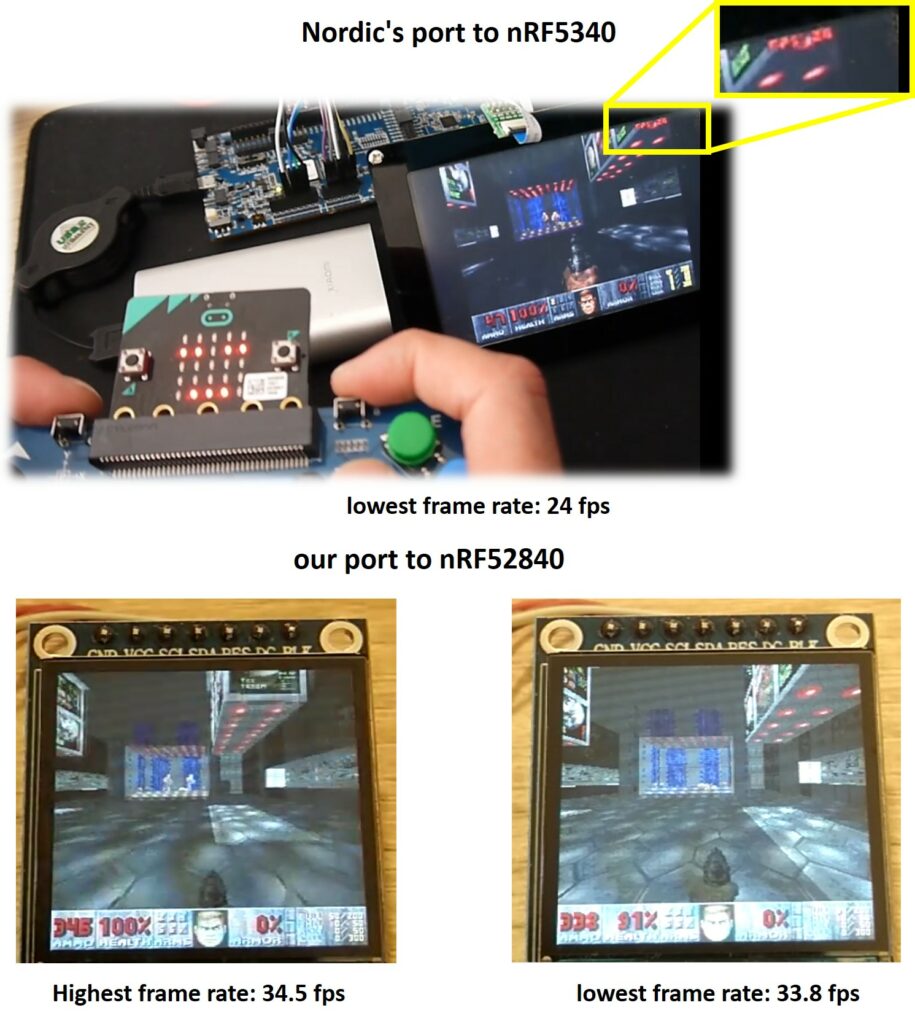
Our port keeps high performances in all the other levels of all the three episodes of the original Doom, even in E1M2, which was one of the slowest maps.
Furthermore the Nordic setup used an FT810, which will take care in converting the 8 bpp image to 16 bpp image. This has two side effect: first fewer bits need to be sent via SPI, therefore the hardware frame rate cap is much higher than 35 fps. Second, since no 8 to 16 bit conversion is required, some hundreds of thousands of CPU clock cycles are saved. In our case it would be about 220 thousands CPU cycles per frame, accounting for more than 3.4 ms. These 3.4 ms correspond to the difference of running at only 30.8 fps and running at 34.5 fps.
With all said, we can state that our port is much more optimized than Nordic one. Still their port support demo playback: demo compatibility is broken in ours. Furthermore, they have implemented a Bluetooth keyboard, where ours wireless gamepad is a very rudimentary one. Still, the nRF5340 has two cores, with the slowest one is already 20% faster than the nRF52840 (considering the differnt DMIPS/MHz values), and that core can be used to handle VERY comfortably the Bluetooth stack.
1993-era PC
What about the comparison with a Doom-era PC?
This page (https://www.complang.tuwien.ac.at/misc/doombench.html) provides an extensive list of different machines with different frame rates, achieved using demo3 (E1M7, hurt me plenty). Unfortunately, our port does not support demo, so an apple by apple comparison is not possible.
However, considerations can still be drawn. Noticeably, in the aforementioned doombench website, results are reported by considering the default screen size, which is 2 levels below the maximum, i.e. the status bar is visible and there is one level of border. This means a resolution of 288 x 144, i.e. only 83% the number of 3D pixels we have in our device.
Therefore, we tried to mimic the demo3, by actually playing the E1M7 level at the “hurt me plenty” difficult level, as discussed above. In such level our minimum achieved frame rate was 27.5 fps. Noticeably, that slow frame rate was achieved only briefly, when lots of sprites were on-screen, and with many sounds being played concurrently (as discussed in Appendix D audio takes some milliseconds. When there is silence, the performance is therefore better). Instead, for the majority of the time the frame rate capped at 34.5 fps. This means that the average frame rate is for sure higher than 27.5 fps. Therefore, not even counting that our resolution was larger, and considering our bottom frame rate value, we can safely state that we run faster than many 486-66 MHz configurations listed on that website. If we also consider that our resolution is 20% larger (1/83% = 120%), we should compare our result with those machines achieving on average 33 fps (i.e. dividing 27.5 by 83%). Furthermore, as we waid above, our frame rate was most of the time capped at 34.5 fps, so we can conservatively state that our gameplay had an average frame rate of 30 fps. Considering the different screen size, for a fair comparison, 30 fps on our device are equivalent with 36 fps on the default screen size mentioed above. Therefore, not only our port on the nRF52840 is faster than almost all 486-66 MHz configuration, but also it is faster than some Pentium-class configurations as well.
This should not be surprising, because from several sources (see [4]) we can infer that a CM4@64 MHz is much more powerful than a 486@66MHz. However, raw processing speed is just only one factor, because data access speed and latency play a crucial role, and a 486 based PC could get better performances in some cases. In fact, the a 486DX2 also had data cache (missing on the CM4), and all the graphics data were copied to RAM, where the throughput could be about 30 MB/s on a 486 DX2 @66 MHz, and with about a 130-ns latency. By comparison, our external flash has a peak speed of 16 MB/s, and an access time larger than 4us.
The Pregnancy-Test Port…
Unfortunately, after one year, there are still people that believe that Doom was actually ported to a pregnancy test. It wasn’t, as one could realize by spending just a minute on fact-checking, reading the original author’s own tweets.
Not only the internal hardware was completely replaced (an OLED display was added, and a Teensy 3.2 board was used, which features a 72 MHz CM4. Of the pregnancy test, only the original plastic case was kept), but also Doom itself was not even running on the new microcontroller. Instead, Doom was running on a PC and the scaled and dithered video was sent in real time through the USB to the Teensy Board, which was driving the display.
Since the display was only a monochrome 128×32 pixel, the entire frame buffer (512 bytes, 1 bit per pixel) could have been sent via virtual COM port with a very high frame rate. Finally the bluetooth keyboard was connected to the PC running Doom, and not to the Teensy board as people believed.
In our case, instead, we did not replace the microcontroller. We simply added a QSPI flash (which acts as the game cartridge of an old-style gaming console, or an HD on a PC) and a display (it is like adding a monitor/television to a PC/console). Some minimal glue logic had to be added as well: a dual edge triggered D-type flip-flop, a couple of diodes and a resistor (these to implement a “AND” logic function). These last additions were required to actually simplify modding. In fact, we could have desoldered the microcontroller, connected two more I/O with very thin wires, and soldered back the MCU to the board. This hard-core modding would have been much more difficult, with respect to just adding an IC and few more components, and a lot of trial-error would have been required as well even on our side. If you feel very brave, you can try this possible solution by yourself, but we cannot guarantee it will work at the first shot. Instead, by following our route, anyone with basic soldering skills will succeed at the first attempt.
That said, even if the pregnancy test was not actually a port (but rather a low resolution “USB monitor”) our device features a bigger display, it is fast and supports sound too. Incidentally, our MCU has even a slower clock with respect to the one powering the Teensy 3.2! (we have more memory, though).
Source and Schematics Download
Here is the github link of the project: https://github.com/next-hack/nRF52840Doom.
In that repository you will find:
- Schematics as found in this article.
- Source code of the Doom port to the nRF52840 (by default this code is set up for the BLE Dongle. In main.h you can easily witch to Adafruit CLUE)
- Source code of the Wireless Gamepad + Audio
- Source code of the WAD Converter
We decided not to provide any pre-converted WAD. Doom WADs can be easily found with a simple Google search. You must then convert them with our WAD converter. Note that we only tried the Shareware, the commercial, The Ultimate Doom and Doom 2 WADs. Other wads (i.e. from expansion packs) are not tested and might not work.
Conclusions
We think we set another milestone. Not only we satisfied all the challenge constraints, but we largely exceeded our expectations. We were also able to run The Ultimate Doom (episode 4 is quite slow, but still completely playable) and all the levels of Doom 2, despite they are more memory hungry. The original Doom and Doom 2 levels are running very fast on this 64-MHz Cortex M4, with only 256kB RAM: for most of the time, the frame rate well exceeds the 30 fps mark, capping at 34.5 fps.
It is worth noting that even if we have only 256 kB RAM, we also have 1MB flash, which can contain constant data and can be randomly accessed at a noticeable speed. It is like if we had a PC with 1.25 MB RAM, because on a PC, even constant data and code (which on the MCU can stay on flash) must be loaded to RAM.
This port will allow running Doom also on hundreds of off-the-shelf devices, as the nRF52840 is used in wireless mices, keyboards, and many other IoT devices. We can’t wait seeing your ports!
Finally one more thought. The performance we achieved here show that in an everyday device as simple and cheap as a Bluetooth dongle you might find a processor more powerful than a $1500 PC you would have played Doom in 1993.
However, make no mistake, this is not (entirely) because of bad programming or lazy software engineers: IoT devices might require an average computing power which is ludicrously modest, however, in order to have them processing/sending data quickly, with a somewhat complex protocol like BLE or Zigbee – and to make them go in sleep mode as soon as possible to save power – you need a peak raw computing power incredibly high as well.
Disclaimer
This project has been developed independentl and with no commercial purposes. You are free to use any information we provided at your risk.
We are neither affiliated to Nordic Semiconductor, nor Adafruit Industries, nor with the manufacturer of the BLE dongle.
We did neither request, nor received any financial support from any of the aforementioned companies. We have contacted the BLE dongle manufacturer, and got the permission to disclose the dongle model number and the link to the store where we bought it from.
Appendices
To make the article easier to read, we decided to separate and put here some insights, analysis, etc., that would break too much the train of thought if left in the main body.
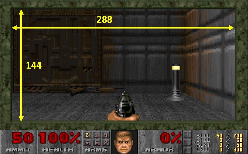
Appendix A: Resolution in Terms of 3D Pixels
In the article we often cite the number of 3D pixels, because the most time-consuming part is the 3D scene rendering, especially on complex maps. When we count the number 3D pixels, we consider only the 3D viewport, i.e. the screen not taking into account the 32-pixel tall status bar. If Doom runs in low-detail mode, each 3D pixel corresponds to two physical on-screen pixel, therefore the 3D resolution is halved, with respect to that one calculated in high detail mode.
In high detail mode, the 3D resolution is the product between the horizontal resolution and the difference between vertical resolution and the status bar height: horizontal_resolution x (vertical_resolution – status_bar_height).
The original Doom screen resolution is 320×200, therefore in high detail mode there are 320×168 = 53760 3D pixels. The Doom port to GBA by doomhack is low-detail mode only, therefore the number of 3D pixels is 240 x 128 / 2 (display resolution of GBA: 240 x 160), i.e. 15360 pixels. Our past project had a display resolution of 160 x 128, but the rendering was in high-detail mode, therefore we had 160 x 96 3D pixel, i.e. 15360 (same as doomhack’s GBA Doom port).
In this project, we used a 240×240-pixel display, in high detail mode. The number of 3D pixel is 240 x 208 i.e. 49920. This is 92% the 3D pixel of the Nordic ports/original Doom, and 3.25 times the number of doomhack’s GBA Doom port and our old project.
Remarkably, with respect to the original Doom screen resolution (i.e. counting also the status bar), with our 240×240 screen we are not that far either: we have 90% of the number of pixels. If we also consider that the default 3D canvas size on Doom is even smaller (9 screen blocks, i.e. 288×144 pixels), then our resolution is ever 12% larger.
Appendix B: Double Buffering, Implementation and Performance Boost
We will first briefly describe how we implemented double buffering, and then we will make some speed considerations.
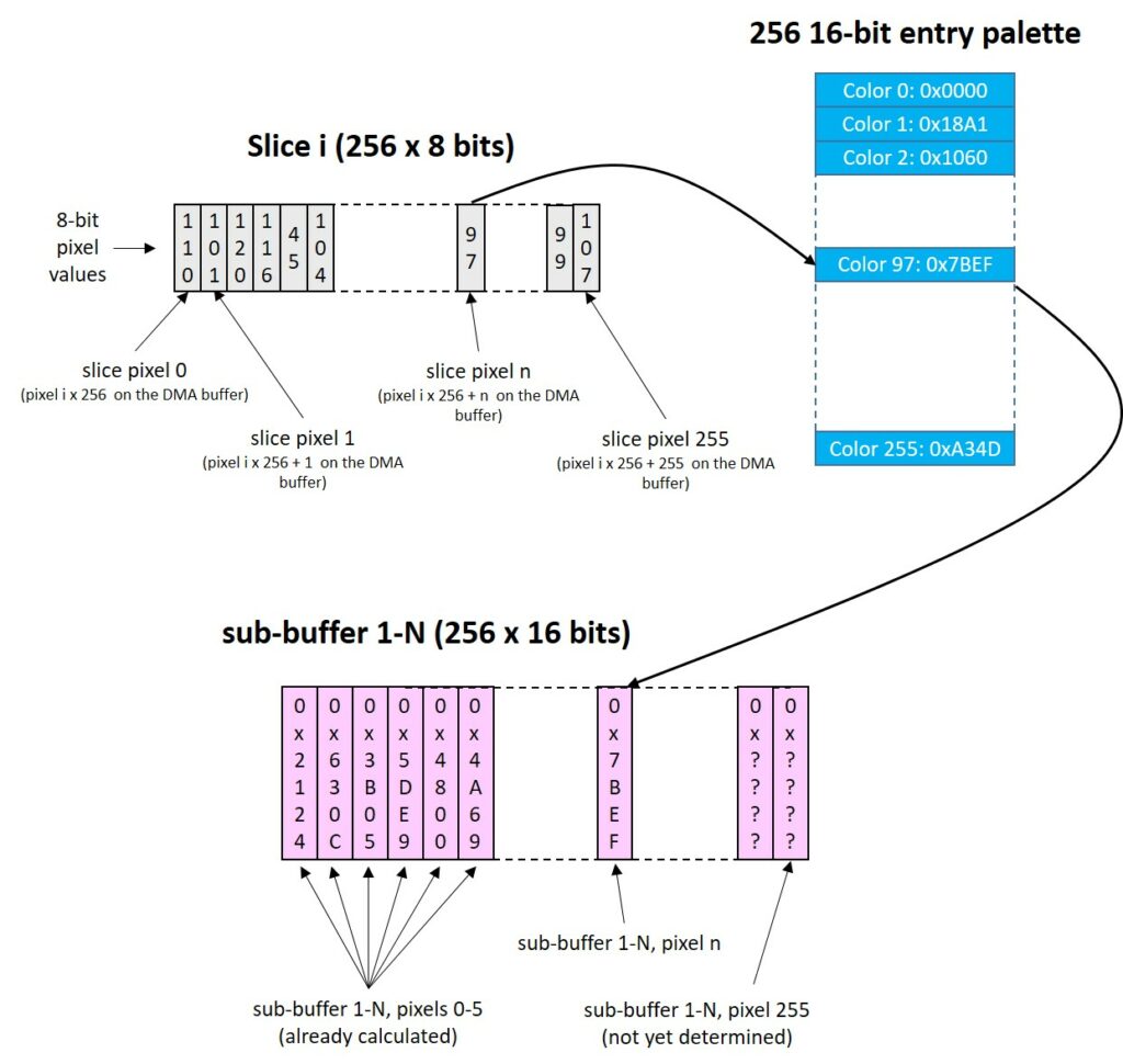
To save RAM, and since Doom uses 8 bits per pixel (256 indexed color mode), both buffers have 240×240 (bytes) bytes. However, the display expects 16 bits per pixel, therefore we cannot directly send to the display the front buffer, but an intermediate step is required.
For this purpose we can logically (i.e. no operation is actually done) reorganize the front buffer in 225 slices, each one 256 pixel large, as shown below. Then, we convert one of these 225 slice at a time.
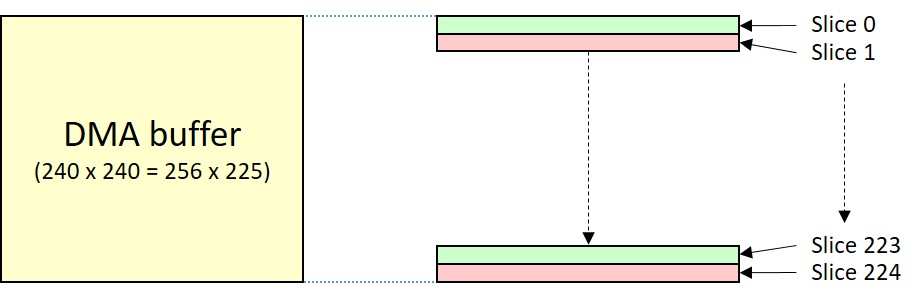
To convert the 8-bit slice data to 16-bit, we use two smaller sub-buffers (yes, another double buffer!), each one containing 256 pixels at 16 bits (512 bytes per buffer). When the DMA is busy sending one of these two 256-pixel buffers, the CPU fills the other with 16-bit values, based on the data of the 8-bit front frame buffer and on the palette. After optimization, this process takes less than 1000 CPU cycles every 256 pixels, i.e. much less than the time the SPI takes to send these 256 x 16 bits, which is 8192 CPU clock cycles (the SPI only goes at half the CPU frequency). When the SPI has finished sending a sub-buffer through DMA, we swap the role of the two sub-buffers. Now the DMA starts sending the sub-buffer prepared before, while we the CPU can fill the other one with the 16-bit values. This process repeats until all the frame has been outputted, i.e. 225 times.
The conversion of these 225 sub buffers takes about 3.5 ms in total. Sending the whole frame data takes about 29 ms (240 x 240 x 16 / 32MHz), therefore, while the DMA is sending data, we have 25.5 ms of spare CPU time, which can be used to actually draw the frame (3D rendering, status bar, menu/hud drawing, etc). If this drawing process is quicker than 25.5ms, then the frame rate will be exactly 34.5 fps. Noticeably, this maximum 34.5 fps is a hardware limit, set by the maximum SPI speed and display resolution. Such maximum frame rate does not perfecly matches the theoretical value (32 MHz / (240 x 240 x 16) i.e. 34.7 fps), because the SPIM3 will introduce a 36-CPU cycle delay between every 256-pixel buffer transmission (therefore each buffer will be sent in 128.56 us and not 128 us, for a total 28926 us per frame). If we take more than 25.5 ms to render the new frame, like in complex 3D scenes, the frame rate will be lower than 34.5 ms.
Now, to understand how beneficial is the double buffering technique, let’s make an example. Let’s suppose that a scene is running at 30 fps, with double buffer. This means that each frame takes 33ms to be calculated, converted and sent to the display. We already said that about 3.5ms are used for 8bpp to 16bpp conversion, therefore in this example the game engine is taking 29.5 ms to create the 3D scene.
Let’s suppose that now we could not use the double buffering, e.g. because we had not enough RAM to implement it. We now need about 29 ms to send the data to the display, as we said above (note that we do not count 8 to 16bpp conversion time because such conversion would now occur, on a pixel by pixel basis, when the previous pixel is being sent to the display). This 29-ms time must be added to the aforementioned 29.5ms 3D rendering time, totaling 58.5 ms. This corresponds to a mere frame rate of 17 fps. In other words, from an excellent 30 fps -achieved with double buffer- we fall down to a mediocre 17 fps.
This also explains why the screen melt effect is playing quite slow. In fact, the screen melt effect is expensive in terms of memory, as you need two frames: the old and the new screen. The old screen melts down and columns of the new one are copied over it, like if the new screen was behind the old being melted. If we used also double buffering, we would require actually 3 frames, i.e. more than 160 kB. As a trade-off, we simply disable double buffering and we use the two buffers to store the new scene, and the old one being melted. Due to this, the minimum frame update time is 29ms, which must be summed to the time required to perform the melting effect.
Appendix C: The Adafruit CLUE as Development Board
To run Doom on the Adafruit CLUE board you need a 16-MByte QSPI flash. Since the stock CLUE board has only a 2-MB flash, you have two options (we tried both, they work well):
- Replacing the built-in 2MB QSPI flash with a bigger one. Do yourself a favor and make sure to get a narrow-body (0.150”) SOIC package. However, if you only have 0.2” SOIC flash ICs (like in our case), you can still manage to solder it on the board, but soldering could be a little tricky.
Note! After you put the new flash IC, the built-in program might not recognize it, and it might indicate QSPI Flash Error. We did not investigate this any further, but we suspect it is because our exact model number comes with the QSPI interface not enabled by default (the flash is put in QSPI mode at run-time in our code), and Adafruit CLUE built-in example code might not have dealt with this case.
- Using a Micro:Bit breakout board, and adding an external flash there.
You will need also a SWD programmer (e.g J-Link) and some sort of connection, to be able to access the SWD data and clock lines, for programming (sorry, no USB bootloader support, it takes precious flash space and it is useless for debug). For this purpose, we used some spring probes and a prototyping board. Note that some careful alignment is required! We also routed contact number 0 and 1 (using a metal spacer and a screw) to route the UART to the JLINK connector. This was useful in debugging the USB CDC stuff.
The block diagram is shown below. As we will discuss later, the low pass filter and port expander are mounted on an external board, using a Micro:bit connector breakout board.
The Adafruit CLUE has plenty of I/O pins on the Micro:bit-compatible edge connector. Creating a gamepad/keyboard for it is easy: you can connect each key to a different GPIO.
Alternatively, you one could use also those 3 digital I-O that accessible with screws and add a shift register or a I2C port expander. Note that our code uses pin 0 and 1 for debug UART, therefore some pin reassignment will be needed.
On the Adafruit CLUE, audio is simple as well. Just pick a GPIO and use it a PWM output, add a simple bypass + low pass filter and you are set. Unfortunately, the PWM generator of this microcontroller is quite limited (in particular the maximum counter frequency of 16MHz is a severe limitation), but we managed to get a good quality nonetheless. The low pass filter is mandatory in this case, because we are pretty close to the human ear sensitivity spectrum.
Noticeably, for the Adafruit CLUE board you can use the wireless gamepad solution as well, which is discussed in the article main body (see gamepad and audio).
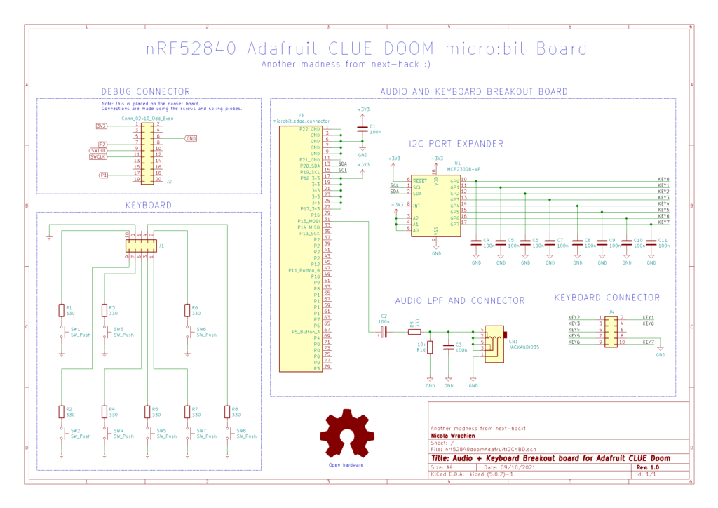
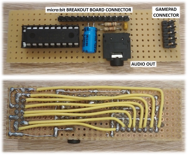
Here is the schematics for the I2C gamepad + audio part, which is connected to the Adafruit CLUE through a micro:bit connector breakout board.
Appendix D: Audio and Wireless Gamepad
The audio subsystem is made of two parts. The first one fills the audio buffer while the second one is responsible of sending the data to the gamepad, via radio. Noticeably, the data calculated in the audio buffer is always fed to the PWM generator (by hardware) even if the wireless gamepad is used. This is to allow us to choose between wireless or locally-generated audio.
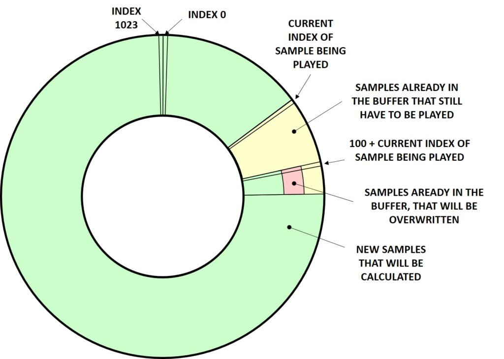
We used a circular audio buffer with 1024 samples of 16 bits, which is filled by the “updateSound()” function, after the 3D scene is rendered.
The audio system supports 8 logic audio channels, which are mixed down to a single one. The updateSound() function will scan all the channels, and for each active one (i.e. where sound must be played), it will first load the audio data from the QSPI flash, and then it will calculate its contribution to the mixed mono-channel output. For each channel, we estimated that loading the samples will take up to about 125 us, while calculating all the contribution will require less than 300us. In the worst case, all 8 channels are active, and the total time taken is less than 3.4 ms.
As we just wrote, loading sound data and calculating all the samples take a quite a long time, therefore we cannot directly update the audio samples starting from the very next sample which is going to be fed to the PWM. Taking into consideration the aforementioned 3.4-ms time, what we can do is to update all the audio samples which will be fed to the PWM at least 3.4 ms after the current one, which is being generated when the updateSound() is called. For this reason, the updateSound() function will get the index of the current sample that is being fed to the PWM, and it will add an offset, called AUDIO_BUFFER_DELAY in the source code, and then, it will update the audio buffer starting from this new index (current index + AUDIO_BUFFER_DELAY). Based on the 3.4 ms time, we should set AUDIO_BUFFER_DELAY at least to 38, however, as we will explain later, to accommodate wireless audio transmission constraints, we set it to 100. This value has the following effects:
- The sound samples calculated by updateSound() will be played about 9ms (i.e. 100/11025 Hz) after updateSound() is actually called. In other words, the time between the triggering of a sound effect and its actual generation increases by 9 ms.
- For an uninterrupted audio signal, updateSound() must be called when there are still at least 100 samples not yet fed to the PWM generator.
- The updateSound() function will update 1024-100 = 924 samples, because the 100 samples after the current index must not be touched, as they still need to be outputted.
Now, since we are generating every time 924 new samples, we must call updateSound() at least every 924/11025 seconds, i.e. no more than about 83.4 ms can elapse between two updateSound() calls. Being updateSound() called once per frame, this results that, for a glitch-less sound output, the frame rate must be at least 12 fps. This frame rate is very unplayable, and thanks to the optimizations it has been never reached in our tests, even when the menu is displayed.
If updateSound() is called more frequently than 12 times a second (this is always true), then some of the samples in the audio buffer are recalculated again, and if there are no new triggered sounds, the overwritten values (i.e. the values that were already ready previously) won’t change. This is quite inefficient, but it simplifies a lot the whole sound generation.
The following diagram shows the representation (not to scale) of the circular audio buffer. The function updateSound() will update all the audio samples, having an index of 100 + the current index of the sample being output by the PWM, when the function was called. These samples are marked in green in the diagram. Samples marked in yellow and red are those calculated previously. The yellow ones will be output by the PWM, however the red ones are those that will be overwritten by updateSound() before they are fed to the PWM, if the frame rate is higher than 12 fps.
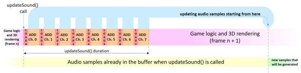
Below we are showing the same concept, “unrolling” the audio buffer, and showing when the updateSound() function are called. Noticeably the diagram below, we are considering that no wireless gamepad is used.
Now, let’s understand why we need an AUDIO_BUFFER_DELAY value of 100 samples, instead of just 38.
This is due to the audio wireless streaming algorithm. The size of each audio packet is a tradeoff of speed and audio delay, as it will be clear soon.
Each audio packet is built during an ISR which is generated by a timer, and it is called about every 50 samples (about 4.5 ms). Each packet will contain 52 audio samples, and not only 50, to ensure that no audio stream interruption occurs due to mismatch in clock frequencies or due to other latencies. This 2-sample overhead allows for about 200 us of buffering time between two packets: an eternity in terms of MCU time.
When the ISR is called, it will take from the audio buffer, generated by updateSound(), the aforementioned 52 audio samples. However, these 52 audio samples must not be overwritten by updateSound() just after the ISR is called, because this would mean that the wireless audio stream has lost some samples.
The following diagram explain this, showing the worst case, i.e. when the ISR is called just before the contribution of last channel (Ch.7) is added to the audio buffer. In fact, when the ISR is called, about 3 ms have passed since updateSound() started updating the samples. As said before, the position of these samples to be updated begin at the sample index that was being fed to the PWM when the function was called, increased by AUDIO_BUFFER_DELAY. Without loss of any generality, we can assume that the sample index that was being fed to the PWM when the function was called is zero. When the ISR is called, the index of the current PWM sample is therefore 3 ms x 11025 Hz = 34. From such index, the ISR will get 52 audio samples, totaling 86, therefore samples between indexex 0 and 85 shall not be touched by updateSound(). Still the aforementioned 3-ms time is just an estimation, based on analyzing the assembly output and time measurements, therefore there might be some uncertainty. As a result, instead of setting AUDIO_BUFFER_DELAY to 86, we set it to 100, to ensure a good safety margin.
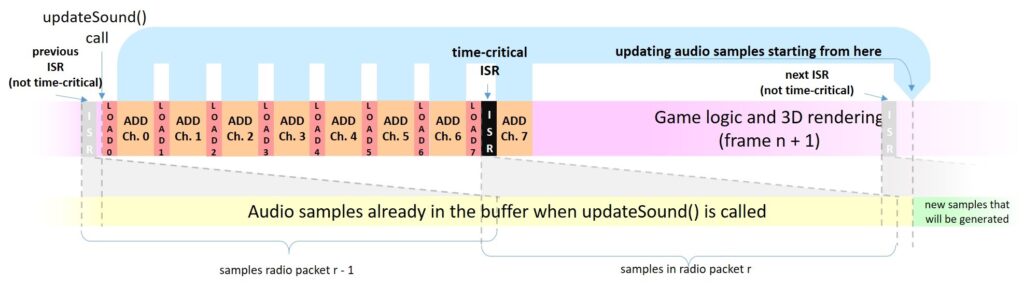
In the same diagram, we also shown two more ISR calls, one occurring before the time-critical one (shown in black) and one occurring after the critical one. Noticeably the overlap between the audio samples in the packet is shown as well, however do not confuse the audio samples that will be put in the radio packet with the time actually taken by the radio to send them! In fact, the radio is sending the 52 16-bit samples at 1Mbps, that is in less than 1 ms, without CPU intervention, therefore each radio packet is well spaced in time.
Now that we have discussed the transmission, let’s get the reception side.
The gamepad will always be in RX mode (slave device), and when an audio packet is received from the master device (nRF52840), it will write on its circular buffer, with a similar technique used for the PWM, discussed above: the current audio sample index being fed to the PWM is added to a delay, and update starts from this computed index. This is to ensure that we are not feeding to the PWM (which is implemented using a timer and the PPI unit) the same samples we are updating.
After the audio packet is received and the samples have been updated, the radio is switched in TX mode and the state of the 8 keys are sent using two bytes: one byte is the bitwise negation of the other. In the meantime the nRF52840 running Doom already switched from TX to RX mode, to get the key status. We are sending two bytes, so that if an error occur, the key status is not updated. Since in one frame (29ms at minimum) we send between 6 and 7 key updates, we are quite sure that during a frame the key status are correctly sent to the nRF52840, so gameplay will not be affected by noise. We have used this dirty trick because CRC is quite broken on the nRF52840. We did not bother implementing the workarounds suggested by Nordic’s Erratas, it was not worth our time for 2 bytes.
Noticeably, the nRF52840 running Doom will be switched to TX mode even if no data packet has been received, by the same ISR that is responsible of crafting the wireless audio packet.
What about error detection in audio? We do not do any error detection. Since our algorithm does implement any audio packet resend feature, and discarding one audio packet due to a single bit flip would create a huge 4.5-ms unpleasant glitch. Instead, a single bit flip can be tolerated, as it lasts less than 100 us, and it is also partially filtered.
What happens if no audio packet is received for a “long” time ? (10 ms). We have implemented a monostable timer, that it is reset every time a radio packet is received. If no radio packet is received before the timer reaches the 10-ms timeout, the audio buffer is reset to the “mute” level. This prevents the generation of nasty noises when the nRF52840 running Doom is turned off, or it is out of range.
Finally, the RF performance are quite affected by all the wires and components close to the antenna of both devices (nRF52840 and nRF51822), as well as the usage of GPIOs, which are recommended to run only at low speed (to prevent RF performance degradation). However, with 1 mW of output power, a decently usable range can be still achieved: after all, no one is going to play Doom on a 1.3” sized display, at a 10-m distance.
Appendix E: QSPI Performance Evaluation and Optimization
As said in the main body, this microcontroller features a QSPI peripheral which allows to treat the external flash as if it was simply an extension of the internal one. However, we soon realized that it suffers a lot from random (or better, non-sequential) read. The performance of non-sequential read are very important, as we are going to discuss now, before showing some actual test results.
Without entering too much into details, the 3D rendering of walls and sprites occurs by column. If sprites/walls are at a distance for which they are not drawn at 1:1 scale on-screen (almost always), then some column pixels need to be repeated or skipped. When column pixels need to be repeated, this is not a big issue. However, if they need to be skipped, the QSPI controller might have to set a new address very often (QSPI memories are optimized for sequential reads and they automatically increment the internal address pointer after each byte). Generally, setting a new address on QSPI memories is extremely expensive in terms of throughput, and in fact we found that loading the entire column (i.e. sequential read) on a local RAM buffer, and then drawing that column is typically much faster than directly fetching the required pixels from the QSPI flash, despite we need first to copy the entire column to RAM.
This is quite understandable. When we read an entire column to a RAM buffer using DMA, we get close (if the column data is large enough to neglect any overhead) to the 16MB/s, because read is done sequentially. Then we can random read that buffer, with a very low latency (A LDRB instruction takes 2 cycles from the 0-wait state RAM). Instead, if we had to random read directly from the QSPI flash, we will have to set many times a new address.
Knowing how much is the delay introduced by random QSPI accesses is important or optimization, but, unfortunately, the Nordic product specification document does not show any details underlying the QSPI, DMA, etc. Therefore, the only way to assess QSPI performance was by actually performing some tests.
The whole analysis is beyond the scope of this article, so we briefly show the results without going too much into the details.
We performed the following tests. Each one was done for various read sizes, between 1 and 2048 bytes
- Contiguous read mode:
- memcpy
- byte copy (starting from the same address as memcpy)
- byte copy (starting from a different address with respect to memcpy. This is offset by 4096 bytes)
- word (4 bytes at once) copy
- DMA read.
- Noncontiguous mode: the source address is incremented by some quantity: 1, 2, 3, 4, 5, 6, 7, 8, 1025.
The QSPI settings are: 32 MHz, no delays, 24 bit addressing mode, code executed from internal flash, cache enabled.
We plot the results both in terms of average latency and maximum throughput, so both small and large values can be appreciated: the read speed in MB/s is calculated as 64MHz/average latency.
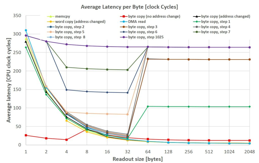
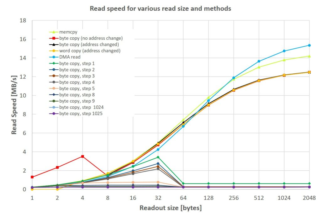
The results take into account not only the timing by the QSPI itself, but also the timing required by the load/store instructions, as well as any setup. The code is available in the main.c. To reproduce the results just set to 1 ENABLE_TESTS.
A complete analysis of the QSPI would deserve a separate article on its own, but what we found is:
- The maximum DMA read speed is quite far off the theoretical one, shown in the datasheet, unless you consider ludicrously high data sizes. For instance, with 2048 bytes we get at most 15.3 MB/s. However, typically a texture column is between 32 and 128 pixel high (there are even smaller ones, but these represent a minority, and optimizing for them would not lead to noticeable boosts), therefore, the actual read speed we expect is between 4.3 and 9.8 MB/s. This is due to the high initial access time we observed also in the other tests.
- “Random reads” have an extremely high latency, which is much larger than what one might expect by reading the datasheet. In fact, from the 4-IO fast read timing diagram shown below (taken from the nRF52840 product specification 1.5), one might expect that a random read (i.e. where the controller needs to set the address) takes 22 QSPI clock cycles, i.e. 44 CPU clock cycles. Instead, we get more than 275 clock cycles for single-byte random reads, i.e. about 4.5 microsecond. This is quite surprising, and we tried to see if we set something wrong. However, in the Nordic support website, we found exactly similar timings by a Nordic employee here in reply to a query about QSPI latency.
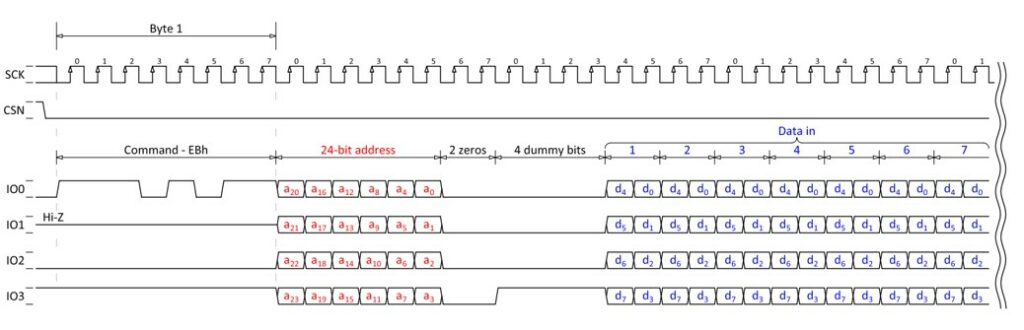
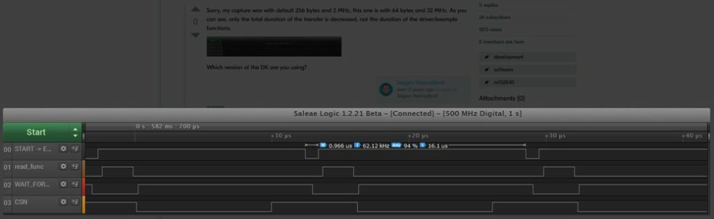
- Reads with step 8 or larger will behave like random reads, i.e. where the step is 1025 bytes (the odd-number was taken to assess if there is some alignment penalty. We found no difference
A completely different scenario occurs with multi-byte reads (word reads). The function memcpy (optimized for performance) also will try to read in 4-byte words if possible (as many as 8 words, using an LDM – load multiple register- instruction), and this explains why it performs the fastest up to 128 bytes.
After 128 bytes, DMA performs better. This is due because the DMA will always check for the QSPI Flash status register, an operation that adds between 0.5us and 1us time penalty, that’s why software (memory-mapped) sequential readout performs better for smaller sizes.
Based on such findings, we decided to reduce as much as possible random reads to external flash, and we used DMA to be able to render each column while next one is being fetched. Even if memcpy performs better for smaller data read, we still used DMA, when we need to cache the column offset array for masked textures and for sprites. In fact, such array is typically quite big, being 4 times the width of the patch to be drawn. If the patch has a width of 32 or larger, then using DMA instead of memcpy will either have little impact, or it will be faster.
Appendix F: Caching and Flash Lifetime
Putting as much data in flash as possible has a dramatic speed enhancement. This has however a major drawback: flash lifetime. In fact, flash memory has a limited number of erase-write cycles (10000 as reported in the datasheet), above which the manufacturer will not guarantee the 10-year retention time. However, this information shall be taken with a grain of salt. In fact, our programming algorithm will always check if we want to write a DIFFERENT data to the same flash page. If a different word is found, then the whole page is erased and reprogrammed. Otherwise, no erase/program operation occur, saving the flash lifetime. Furthermore, data typically changes only when you change level, i.e. if you start the same level no erase/program operation will be issued.
This means you need to change level 10000 times, before your microcontroller MIGHT not retain data for 10 years. These numbers are well beyond any reasonable usage. Beside this, the code-section is not touched, therefore only the data section might change.
Appendix G: Openings
An opening is the separation between regions of solid and transparent pixels on a column. Original Doom defined 64 x 320 openings, that means that on average up to 64 openings could be on each horizontal column. Noticeably, saying 64 openings per column does not mean that you can’t have more than 64 openings on one column: you can exceed that number, but there will be simply less openings available for the other columns.
It is worth to remark that an average 64 openings per column is very hard to achieve. Actually, we found no issues also with a lot of less openings.
On his port to the GBA, doomhack set the limit to only 16 openings per column: with this limit, we did not find any issue with all the Ultimate Doom maps, so we used this value as well. We also found that the original Doom shareware episode had no issues with only 8 openings per column. However, we did not try the other episodes with less than 16 openings per column.
Appendix H: Hardware and Software Video Gamma Settings
The default ST7789 gamma settings create a too bright image, partially losing the original look and feel. Therefore we have tweaked the gamma settings to be quasi linear curve, in order to match more closely what you might expect using a PC. You can choose the two gamma curves at compile time (hardware gamma settings), by setting to 1 the symbol “GAMMA_CORRECTION” in main.h. You can still get brighter images by changing – during game- the gamma level (software gamma settings).
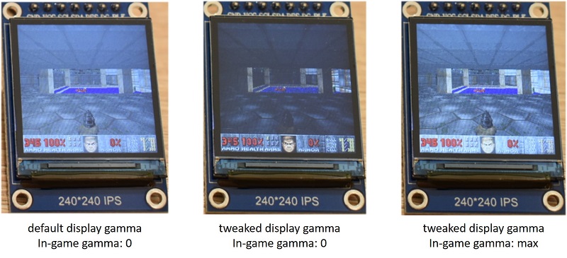
When taking pictures shooting the video we used the modified gamma curve, but with an increased software in-game gamma settings. These still look better than using the default ST7789 gamma settings with no gamma correction.
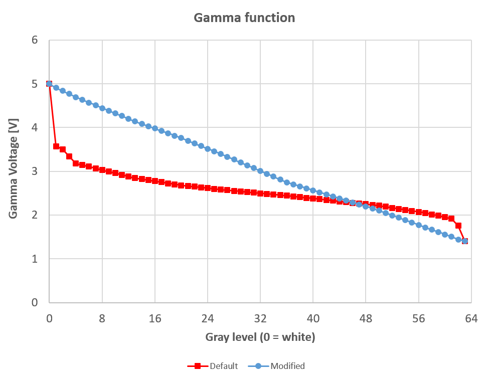
[1] This was done also because the GBA allows for a nice trick. If you write just an 8-bit value to the video memory (which is 16-bit wide), then the upper byte is written as well, with the same value of the lower one, meaning that with one write, you have the other for free. This is useful because the GBA port by doomhack use low detail mode (one 3D pixel is 2 “real” pixels wide).
[2] According to Segger, you do not need to be a student to buy and use a Segger EDU, but you shall not use it for commercial project. This is an open-source do it yourself project, so you can use it.
[3] When the frame rate is either software-limited (frame rate cap), or hardware-limited (e.g. when the SPI cannot update a screen any faster), we can only state that the device is capable of running at least at that particular limit. However, we cannot determine if, without that software- or hardware-limit, the device could have run at faster frame rate, unless we measure the “idle” time (i.e. when the device is waiting either for a tick – 1/35 second – to elapse, or when the device is waiting for DMA operation to finish, before start sending the new frame to the display). That’s why comparisons must be done when the frame rate is below the limit, hardware or software.
[4] ARM states that the CM4 has about 1.25 DMIPS/MHz and 3.43 CoreMark/MHz. In their datasheet Nordic states that the nRF52840’s performance is 3.3 CoreMark/MHz, which is quite close. By searching “80486” on https://www.eembc.org/coremark/scores.php, we find that the a 486DX2 @66 MHz scores only 1.02 CoreMark/MHz. An Intel Pentium features 2.14 CoreMark/MHz. These data suggests our device could be as fast as a 100MHz Pentium.
[5] Our maximum frame rate is 34.5 which is rounded to 35 (on Nordic’s port the frame rate is shown without decimal part).
Pingback: Doom ported to small nRF52840-based devices including the Adafruit CLUE at 30fps #CLUE #DOOM @Nordictweets @next_hack « Adafruit Industries – Makers, hackers, artists, designers and engineers!
The nRF52840 DK does has a QSPI flash, and it was used for the Doom port. I remember having to work around a hardware bug in the revision of the chip I used, where I had to insert a bunch of NOPs after every XIP/memory-mapped access to QSPI memory.. not fun. The reason it was so slow and lacking wall textures was mainly because I hadn’t made much progress yet and hadn’t started optimizing. Moving to nRF5340 was always the plan. I think it was running a bit better than what’s showed in the video when I made the switch to nRF5340.. maybe 10-12fps.
I don’t think you mentioned it, but the nRF5340 has a decent cache between the CPU and on-chip flash NVM and QSPI memory. When I got the nRF5340 port compiled, and boosted the CPU clock up to 128Mhz I got little boost in fps. Then I enabled the cache and got a big boost up to ~30fps. That cache makes everything so much easier. After that it was just back and forth between adding graphics/features and optimizing to stay within the memory limits and keeping fps high.
I remember thinking it should be possible to run Doom on nRF52840 pretty well. But it felt like there’s a threshold where, at 256kB RAM, running a fully featured version of Doom is possible, but incredibly hard. While at 512kB it’s almost easy. Given that you have a few megabytes of ROM/NVM/etc. with half-decent bandwidth of course.
For all the talk of Doom running on everything, I was surprised how few high fidelity ports there are to memory constrained devices. Before this port, the GBA port was the one that impressed me the most. But this is now the most impressive one IMO. Incredible work.
Also, I must say, what a fantastic and technically detailed write-up!
If you use the same display as the nRF5340-port I guess full resolution at acceptable FPS should be possible. One can argue whether it’s cheating to have the display driver do colormap lookup. Do you know if this was done by the CPU or hardware on a 486? Anyway, the challenge would be to fit the framebuffer in RAM. Maybe do some lightweight compression?
I might borrow some of the optimizations if I ever get back to improving the nRF5340 port. Hope that’s OK. Gotta make room to add multiplayer and music. Loading some of the data to internal flash is a good idea. I had the thought, but wanted to keep loading times short, since development time was limited. I would never had thought to optimize code for size, except performance critical ones though, to have more space for data. Brilliant!
Hi,
thanks for the corrections and compliments!
About data cache, we had verified on an STM32H743 (downclocked) that data cache has tremendous effects on the frame rate indeed. Instruction cache almost had no change with data cache off. This is probably that still the CPU was waiting for the data from the memory mapped QSPI.
The FDTI is not cheating in our opinion, in fact if we recall correctly, also the original Doom used an 8-bit palettized mode (i.e. hardware conversion between 8 bit and 24 bit). We will use a similar trick on our next port, because next target has an even slower SPI, so saving 2x in bandwidth will make huge difference. In this port we did not want to use such device, because we wanted to add the smallest number of components, so we did this conversion in software (interrupt).
Borrowing optimizations is ok: the project is open source 😉
cheers!
Wow, that’s pretty cool 🙂
BTW, you can also get similar dongle with most 52840 pins available –
the E104-BT5040U https://www.aliexpress.com/item/1005001529756677.html
Thanks 🙂
Yes you can also get nordics’s nRF52840 dongle for a similar price, but one of the points of the project was to port Doom to some off-the-shelf device, and not to a dev board. For instance, we know that some logitech mice use the same MCU, but these were too much expensive for the project.